1 Application
In this application, we will create a high-speed counter which is used to increment the NCO register. The NCO will increment as long as an external pulse signal is high. This creates a high-resolution, long-duration counter, as the NCO counter is a 20-bit wide register. It will take approximately 16 instruction cycles (4 μs with 16 MHz clock) for the data to be read and the counter to reset, so it is necessary to have at least 4 μs of low time between pulses. A falling edge interrupt flag on CLC2 provides a signal that the pulse width measurement has been completed. While the NCO register has been designed to be resistant to glitches on the clock input, it is still good design practice to have clean signals feeding into the NCO clock line.
In order to implement this technique, the PIC16F18076 device was used because it has four CLC modules and an NCO module. Three of the CLC modules are used to create the glitch-free clock, which is ultimately sent to the NCO module. The remaining CLC module routes the internal FOSC to the RC4 pin so that it can be viewed with a logic analyzer. Other signals internal to the CLC (XOR output, latch output) have been brought out to external pins to provide greater visibility of how the application is functioning.
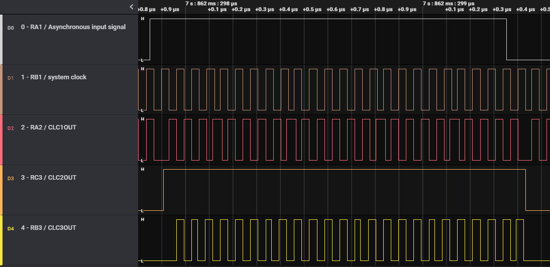
The block diagram (Figure 1-1) shows the asynchronous input signal on RA1, with the CLC outputs feeding the logic analyzer. The CLC3OUT signal is our glitch-free clock signal and is being fed into the NCO1CLK pad.
The first design for this circuit does allow glitches to pass in, and is a simple AND of the pulse signal with the system clock. Note how a spike (red box in Figure 1-2) on the clock is created when the pulse signal rises shortly before the clock falls.
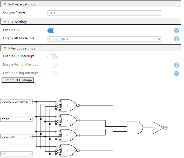
We want to use the AND function to clock the NCO when the pulse is high, but we would like to get rid of the glitches on the clock signal. In order to do this, it would be ideal to create a pulse. This pulse is a new signal that would only rise on the rising edge of the clock, and only fall on the falling edge of the clock. This new signal (CLC2OUT) can be ANDed with the oscillator clock, and there will never be a glitch on the NCO clock signal. The output for this new signal will be high if the data is high on the rising edge of the clock. The output for this new signal will be low if the data is low on the falling edge of the clock.
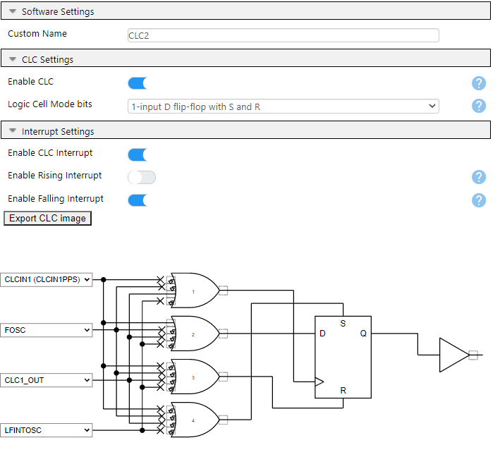
This can be implemented with a D flip-flop and an XOR gate. The XOR gate will have the function of taking feedback from the D flip-flop and inverting the clock, so that it will trigger on the falling edge once the flip-flop has been set. A schematic for this is shown below (Figure 1-3).
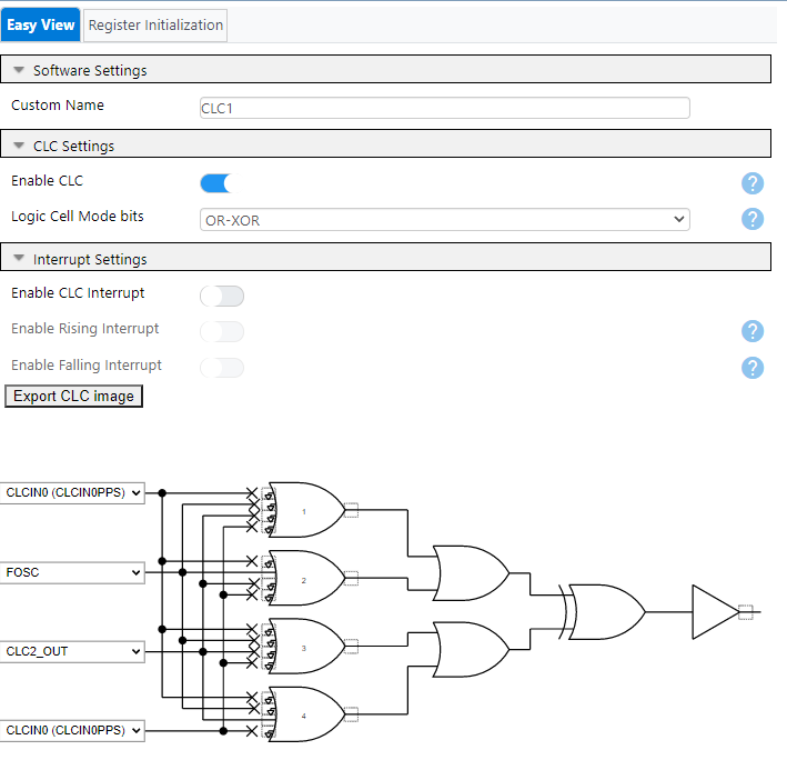
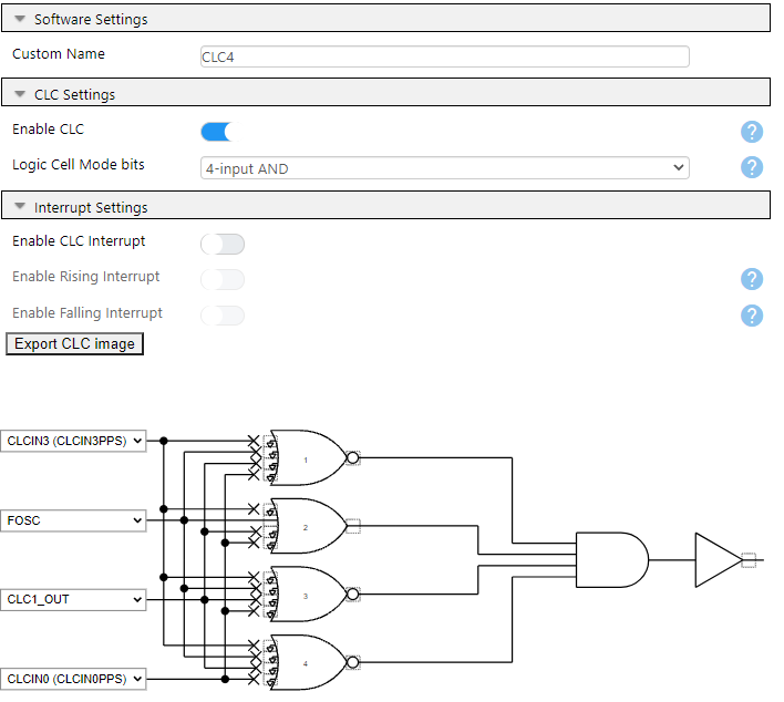
The schematic has been broken down so that each logic function will use one CLC module, and the following images show how the schematic is implemented using the CLC modules pages in MCC Melody (Figure 1-4, Figure 1-5, Figure 1-6, Figure 1-7).
