
2 Layout Recommendations
This section includes the layout recommendations split into various groups according to the corresponding theme. Recommendations for general trace layout, Bus Interface Network (BIN) layout, Power and Ground(GND) planes as well as component selection are made.
Trace Layout
- Ensure consistent impedance is achieved for impedance controlled signals
- Reduce or eliminate crosstalk between signal lines, power lines, and both types of lines, e.g. isolate signals from possible adjacent crosstalk aggressors by at least five times the signal’s trace width
- Reduce total inductance and loop area, including signal source path and its return current path
- Place power decoupling
capacitors directly below the device to minimize loop area and total
inductance
- One side of the capacitor should be connected to the pad using a via
- The other side of the capacitor is connected directly to GND (Ideally connected directly to the thermal vias connected to the exposed pad of the device)
Figure 2-1. Optimal Placement of Decoupling Capacitors 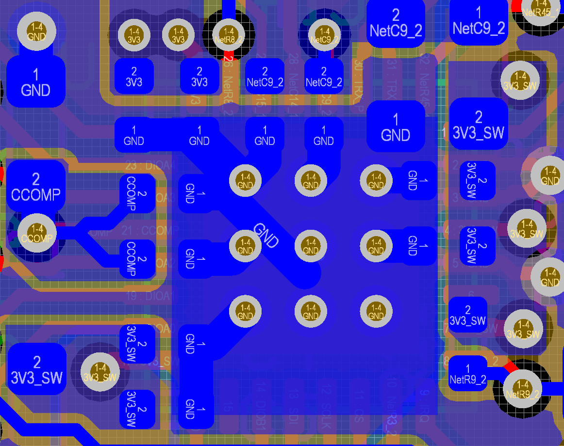
- If the recommendation above is not possible, reduce the loop area and trace length to the decoupling capacitors as much as possible
- Do not share ground pads or vias for decoupling capacitors. Each capacitor must have its own GND pad and via
- For RMII applications, the
trace length of the oscillator to the PHY and to the microcontroller should
have matching lengths to assure the clock signal arrives in both devices
simultaneously. The length matching should be within about ±500 mil. It is
advised to add a series resistor placed close to the oscillator in both
traces to the LAN8670/1/2 and the MCU
Figure 2-2. Optimal Clock Trace Routing 
- Reduce interconnect trace lines on the PCB as much as possible
- If longer distance is required between the device and microcontroller, extend the application interface (MII, RMII, SPI, 3-pin) traces to minimize parasitic capacitance of the BIN connection to remain within the specification, not the BIN including the TRXN/P trace between the PHY/transceiver and network connection
- All serial data signals (MII, RMII, SPI, 3-pin, etc) should be routed over a continuous reference plane, avoiding plane splits and voids in order to minimize ground return loop path and cross-talk within it. Routing over split reference planes increases the loop inductance & can introduce mixing with ground return currents (crosstalk) from other noise sources
- MII/RMII/SPI lines can cause
EMI and be affected by EMI. Use general high speed digital layout
techniques. A 50Ω controlled impedance trace may be required, as well as a
series resistor before the device. Refer to the Reference Schematic section
of a device’s data sheet for additional information.
- There should be a continuous GND reference plane below MII/RMII/SPI traces
- BIN and MII/RMII/SPI circuits should be separated by at least five times the largest trace width of these signals
- BIN and MII/RMII/SPI lines should not be parallel or cross each other where possible. Necessary crossings should be at 90 degrees
- MII/RMII/SPI should not run parallel to power lines to prevent crosstalk
- Ground stitching around SPI lines recommended
BIN
- Reduce the total parasitic capacitance as much as possible
- Keep the trace impedance at 50Ω
The signal frequencies which compose the bandwidth limited signal in a 10BASE‑T1S network lie well below 100 MHz. Assuming a signal propagation speed of around 5‑6 ns/m, the electrical length of a signal transition is around 2m and longer. This is much longer than a typical board interconnect length, meaning that when deciding whether to reduce stray capacity or keep trace impedance strictly at 50Ω, it is often better to reduce capacitance since transmission line effects only begin to show effects at longer distances, at around one tenth of the electrical length of a signal.
- Follow the BIN Application Note AN1718 for schematic and layout where possible
- Increase isolation
(clearance) between BIN traces and GND to reduce stray capacitance
- Prioritize lowering stray capacitance of layout. BIN traces should be short, thus the effects of impedance mismatch are less impactful than added capacitance because the signal is band limited
- Include a cut-out region below the BIN for all layers to reduce capacitance
- Keep trace width as constant as possible, no vias unless truly required
- P and N trace should be equally long, have same number of vias and other trace changes (widening, narrowing, etc.) and distance (clearance) to GND sections in order to balance parasitic capacitances and mode conversion effects
Figure 2-3. BIN Cutout Area 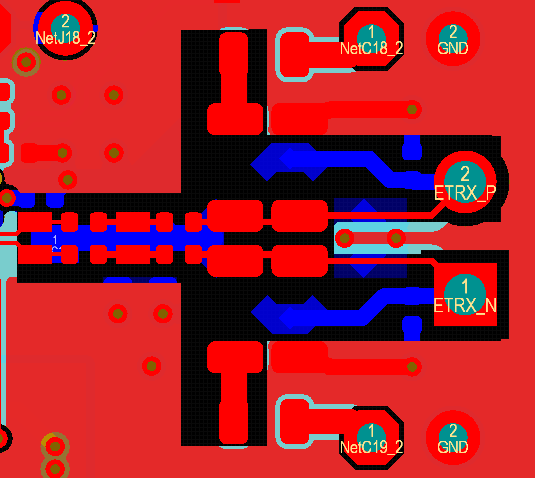
- BIN components connected to GND should be connected to a bulk GND section. Thin traces or vias connecting the components to GND should be avoided
- Reduce stub length of the BIN circuit as much as possible
- Stub length refers to the distance between the T-intersection of the P and N lines of the MDI and the pins on the PHY. The T-intersection can be located on the cables, the connector or the PCB
- To minimize the added capacitance, the T-intersection should be located on the PCB and the traces should be kept as short as possible. Refer to AN1718
- See Figure 2-3 for optimal BIN length
- For BIN, connect ESD protection directly in-line with the BIN trace, reduce trace length as possible. Utilize “flow-through” technique (route trace through ESD device’s footprint)
- Apply flow-through layout for BIN traces to avoid generating extra loading through stubs
- Do not use jumpers or other split-off lines on BIN traces if not shown in the app note. Do not create additional stubs, unpopulated trace forks or T-intersections, as these create additional reflections and degrade signal integrity
- Add any testing points, if possible in-line (on the trace rather than through extra stub)
-
Termination resistors should be placed symmetrically for both the P and N trace. The decoupling capacitor (C3 in the BIN Application Note) in the termination layout must be placed symmetrically to the P and N termination resistors. A trace should connect the common point of the resistors. The decoupling capacitor should be connected to the center point of this connecting trace
Alternatively, two capacitors with half the capacitance can be placed physically close to the termination resistors. The discharging resistor parallel to the capacitors may be placed next to either of the two capacitors
It is imperative that termination resistors and the decoupling capacitor are placed as symmetrically to the P and N traces as possible. This prevents mode conversions from high frequency signals from EMI or steep edges
Figure 2-4. Symmetric Trace Respective to Termination Resistors 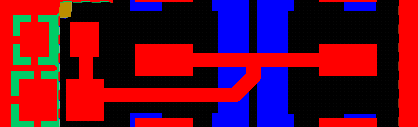
Power/GND
- Accommodate wake and sleep options of the device if desired (WAKE_IN, WAKE_OUT, INH, etc.)
- Provide a low impedance connection to the power grid
- Reduce digital and analog noise to and from other devices on the power grid
- Provide a quick return path and low loop area for high frequency noise with decoupling capacitors
- Connect GND planes together using plenty of regularly spaced vias
- Connect the exposed pad of the device to the ground layer using a via array
- Oscillator GND should be connected directly to bulk GND
- Signal traces must be routed away from power regulator circuitry in order to prevent coupling from the high dI/dt loops
- Power and signal traces should not run parallel
- Include power planes or isolated power islands to provide power supply to the device. These power islands should be separated through ferrite beads and a bulk decoupling capacitor. Refer to the Application Information chapter in the LAN8650/1 and LAN8670/1/2 data sheets
- Trace width for power lanes should be as wide as possible. Power planes or large polygons are preferred over trace routed power. Bulk power areas reduce Power Distribution Network (PDN) impedance and power related noise
Component Selection
When selecting components, it is important to choose the correct size and values. For capacitors, it is important to choose the correct voltage rating as well.
- Correct component selection:
- CMC/DMC/Inductors for Power over Data Line (PoDL) are rated for the maximum current that will be expected
- Capacitors and other components must be rated for the maximum voltage that can occur on the data lines
- Smaller 0402 decoupling capacitors help optimize the layout