
3 Pin Description
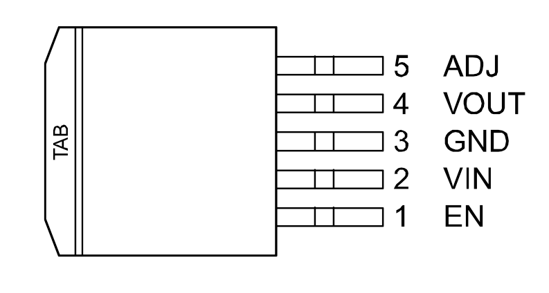
| Pin Number | Pin Name | Pin Function |
|---|---|---|
| 1 | EN | Enable (Input): CMOS compatible input. Logic high = enable, logic low = shutdown. |
| 2 | VIN | Input voltage that supplies current to the output power device. |
| 3 | GND | Ground (TAB is connected to ground on DDPak). |
| 4 | VOUT | Regulator output. |
| 5 | ADJ | Adjustable regulator feedback input. Connect to resistor voltage divider. |