
2.1 2-CLCs Debouncing Solution
Figure 2-1 presents the logic diagram for the 2-CLCs solution. Four 2-input D flip-flops represent two groups of CLCs, CLC3 and CLC1, CLC4 and CLC2 respectively. They correspond to two input buttons, RC5 and RB2, respectively. The input signal of CLC3 is logical AND with the CLC3 output signal to serve as input to CLC1. The timer6 signal serves as clock for all CLCs. The timer can be reused among all the buttons if their debouncing scan rates are in the same range. The debouncing output will light the LEDs (D2, D3, D4, and D5) for demonstration purpose on the MPLAB Curiosity HPC board. PIC18F Q10 family devices contain up to eight CLCs which means four buttons can be supported. The debouncing is performed with hardware peripherals and no code is required other than configuring the timers and CLCs in MPLAB Code Configurator (MCC) in MPLAB X. It does not require external hardware filtering and hence avoids extra space usage and cost. The configuration is explained in the Project Creation and Configuration chapter.
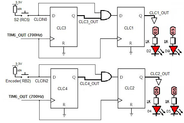
Figure 2-2.a, .b, and .c illustrate the oscilloscope trace of three scenarios when the rotary encoder is switched ON, OFF, and partly switched. In the oscilloscope trace, CH1, the yellow colored signal illustrates the digitized input signal. CH2, the green colored signal, is the debounce signal, which is equivalent to the CLC2 output, CLC2_OUT, in Figure 2-1. As shown, when the encoder gets switched there are many short noisy pulses before it gets stabilized. These noisy pulses normally have a period of maximum 500 μs for the example rotary encoder. In order to filter out these noisy pulses, it is crucial to make sure that the CLC clock period is much larger than the maximum noisy pulse period. This ensures that no noise pulses are recognized as ghost debouncing in two consecutive clocks. A 1.5 ms clock period is chosen in this case, which is three times the maximum noisy period, which means around 700 Hz clock frequency for the timer to overflow. The CLC clock can be configured at any frequency depending on the requirement.
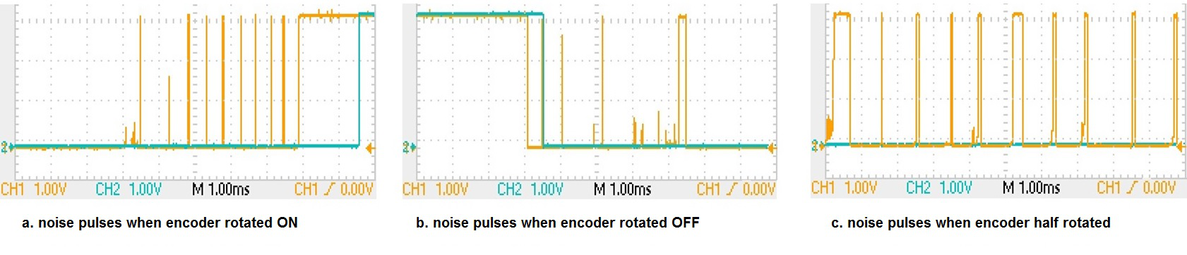
For the 2-CLCs solution, the output signal will be logic HIGH when the input signal is held HIGH consecutively for two clock cycles. Since the noisy pulses in Figure 2-2 all have periods shorter than 500 μs which is smaller than the CLC period (1.5 ms), one noise pulse can get the 1st CLC output signal to be logic HIGH but will not lead the 2nd CLC output signal to be HIGH, and hence no debouncing occurs. Note that the input signal must be low for only one clock cycle for the debounce output signal to go low, as the output debouncing signal is ANDed of the input signal and the 1st CLC output. This is the case for the debouncing signal shown in Figure 2-2.b.
In the extreme case, when the rotary encoder is half switched, the two pieces of metal comes into partly contact for a longer period. The input signal gets very noisy and many noise pulses occur continuously as shown in Figure 2-2.c. In this case, the chance that the input signal is read HIGH at the two consecutive CLC clock cycles increases and debouncing would occur. However, there are still not any debouncing monitored in the oscilloscope for this extreme case. The reason why no debouncing occurs might be due to that the noisy pulses have a much shorter period (<300 μs) than the chosen CLC clock period (1.5 ms). Another important reason is that there are no two consecutive noisy pulses which are caught at the CLC clock edge. The chance still exists though it has not been seen in experiments.