
8.6.4.1 10BASE-T1S PMD Transmitter Characteristics
| Parameter | Symbol | Min | Typ | Max | Units |
Additional |
|---|---|---|---|---|---|---|
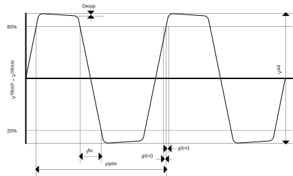
| Differential driver output | Vod | 0.8 | 1.09 | 1.2 | V | Figure 8-11 |
| Cycle-to-cycle jitter |
tj(c-c) | — |
1.04 |
1.2 | ns |
Note 1 |
| Rise time, Fall time (20%-80%) |
trtx, tftx |
7.9 | 10.8 |
14.75 | ns |
Note 1 |
| Droop | 0 | — | 13 | % | ||
|
Notes:
| ||||||
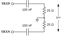
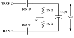
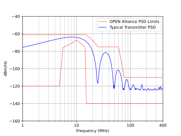
Power spectral density was measured in multidrop mode (50 Ω termination) with the test fixture shown in Figure 8-11 and the transmitter in the IEEE Transmitter PSD mask test mode 3. The upper and lower limits shown are as proposed by the OPEN Alliance TC14 10BASE-T1S System Implementation Specification, Version 1.0.
Topology Discovery
The following section describes the Topology Discovery timing and behavior.
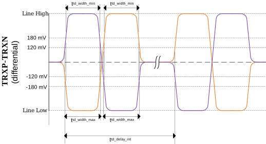
| Parameter | Symbol | Min | Typ | Max | Units |
Additional |
|---|---|---|---|---|---|---|
| Differential Pulse Voltage Amplitude | VTP_diff | 400 | 500 | 600 | mV | Note 1 |
| Width of Topology Discovery Pulse | ttd_width | 49.5 | 50 | 54.7 | ns | Note 1 |
| Minimum total internal delay | ttd_delay_int | 100 | — | — | ns | Note 2 |
| Delay between rising edge on TX and rising/falling edge on MDI | ttd_tx_mdi_dly | 15 | 20 | 30 | ns | Note 1 |
|
Notes:
| ||||||