
3.2 e-Fuse Functionality
The short circuit is a fast event, developing within a hundred ns, and creates an intense transient event that must be carefully mitigated to prevent damage to the power circuitry. Additionally, the short can be mistaken with inrush current, which leads to an increase of mitigation complexity in order to suppress the false-positive outcomes.
If bidirectional circuitry load conditions differ between current flow directions, mitigation becomes more challenging. The dsPIC33 DCS series, accompanied by the AVR SD on the reactive side and the SiC power FETs as solid-state switches, possess all the required characteristics to implement such a solution. This configuration requires a minimum number of additional parts and offers significant flexibility in terms of systems response, as it is fully software-defined. Therefore, the current is mitigated by the main MCU (dsPIC33 DSC) using three parallel loops:
- The first loop uses fast comparators with
adjustable thresholds, rather than traditional ADCs, along with combinational logic
and precise timers. This configuration allows for a repaid response, within tens to
hundreds of ns to effectively manage sudden changes in current flow.
The logical flow consists of the following steps:
Figure 3-2. Short Circuit Walk-Through Logical Flow - Two dsPIC33 DSC internal counters, CNT1 and CNT2, are loaded with the values representing the detection timings for Hard Switching Fault (HSF), a short already in place when the load is turned ON, and Fault Under Load (FUL), when the load gets faulty during the system operation with the FETs already turned ON. The difference between the two is the di/dt which impacts the MOSFETs’ short-circuit withstand time (SCWT). Consequently, the turn-off time depends on the type of short being processed.
- When the short circuit current threshold is exceeded in any direction, the driver enters a weak mode to extend the MOSFETs’ lifespan, and both counters are started. This two-step gate control voltage clamping technique is inspired by the Baliga Short-Circuit Improved (BaSIC) method.
- If the first counter, CNT1 (used for HSF), overflows, the current is measured again. If a new threshold is reached (which assumes a higher di/dt), both MOSFETs are turned OFF.
- If the di/dt is lower, but the system remains in a short condition, the MOSFETs are turned OFF only after CNT2 overflows.
- If the di/dt is lower, and the system is no longer in a short condition, after CNT2 overflows, the MOSFETs weak driving state is turned OFF and the system is set to a walk-through condition.
During nominal operation, when a certain current is established through the load, the short processing chain health condition can be tested as a measure of LFD by temporarily adjusting the comparator thresholds.
- The current data are monitored and primarily used to keep the switcher within its Safe Operating Area (SOA) using a quadratic or higher-order calculation. This calculation can also detect overcurrent, identify arc flash events, estimate signal quality, as well as recognize engagement based on load profile by applying DSP techniques such as FFT, wavelet analysis, in-band power estimation, correlation and inferencing methods.
- The FET Module’s temperature is continuously monitored, and in the event of over temperature, the Solid-State Switch disconnects the load. The module temperature evolution is monitored and compared with the environmental temperature in order to preserve a valid safety case, because high level SIL compliance assumes components are always operating in nominal conditions.
The e-Fuse trip graph, controlled by the main MCU (dsPIC® DSC), is shown in Figure 3-3. The red line represents the border for HSF condition, while the orange line indicates the border for a short under FUL conditions. As observed, the HSF time reaction is the fastest, followed by the FUL, then overcurrent condition and the overtemperature that develops more slowly. The graph lines present the walk-through scenario when the HSF or FUL short is temporary and the systems recover without disconnection, as the e-Fuse shall be immune to false positives. In other words, in the case of each type of short on the left side of the border the system must not trip and on the right side shall trip.
Besides short mitigation, additional functions are essential to meet the SIL level requirements:
As part of Latent Failure Detection (LFD) discovery, another specific function is SSR leakage detection. This function is performed every time the MOSFETs switch ON or OFF. As the current passes by, the FETs are subject to self-heating. If the leakage is measured at two thermal points, during ON to OFF and OFF to ON transitions, ambient (when the transistors are at environmental temperature) and hot (when the FET is right after operation), the ratio between the two values can indicate possible future solid state switch failure.
The patented circuitry can be licensed for usage with our SiC modules and our various MCU-based safety topologies.
Another general function is provided by the supervisory and telemetry data interchange mechanism between the main and reactive sides, comprising of two groups of signals (as shown in Figure 3-4).
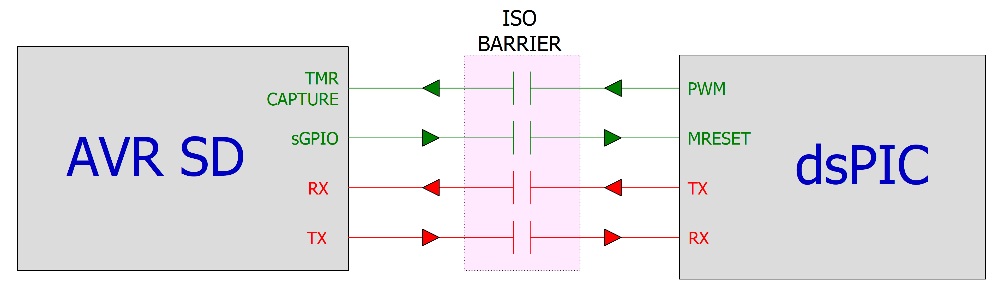
- Watchdog Group (green signals): One of the
roles of the reactive side is to act as watchdog. This means that in case of
malfunctions, a GPIO with safety characteristics can apply a hardware Reset to the
main subsystem. The checking involves a PWM signal generated by the main subsystem
with a modulated duty cycle established by a repetitive sequence of interrupts
called by the running software.
The signal profile allows the reactive subsystem to diagnose main subsystem clock domain issues (e.g., reference clock frequency deviation) or software abnormalities based on pattern recognition. The required MCU resources for the reactive side are: sGPIO (a standard output with safety characteristics for a deterministic state in case of failure) and TMR CAPTURE (a timer capture input that processes the PWM pattern); and for the main subsystem, MRESET (hardware master reset) and PWM (a PWM output that generates the pattern).
sGPIO/ MRESET isolator requires, at the output, a Deterministic Safety State (as an isolator hardware failure shall set the main subsystem in a Reset State, which is the Default Safe State).
- Telemetry Data Exchange (red signals):
This is a bidirectional asynchronous communication using a traditional serial port.
As the data exchange channel is considered gray (not 100% reliable), the data
packets require CRC/ CHECKSUM for verification and a certain sequence in time.
Invalid packets can be dropped, and a similar protocol to AUTOSAR E2E can be
implemented. A standard serial port is used for data interchange: RX (UART
receive) and TX (UART transmit) on the main subsystem and RX (UART
receive) and TX (UART transmit) on the reactive side.
The exchanged payload between subsystems comprises remote health telemetry and measurement cross-validation information.
The reactive subsystem performs the following functions:
- Current Validation Implementation on the
Reactive Side
A possible implementation of the current supervisor uses a Hall effect bidirectional current sensor with a bandwidth of a few hundred kHz to 1MHz, and with a nonlinearity better than ±0.1%. Its isolation capability (kV level) makes it a good candidate to validate (as a secondary measurement unit) if the subsystem that performs the short circuit protection failed irreversibly. Since this type of sensor will only see the average of current, it will not ensure active and non-destructive short circuit mitigation, but it will guarantee load disconnection (within PST) in the case of main subsystem permanent failure.
A circuitry with built-in test is required to ensure that a sensor failure will be eventually detected.
- Load Disconnect Implementation
The load disconnect is accomplished using a physical element with intrinsic characteristics that make it fail in a predictable way, which will always lead to a System Safe State. For this function, consider an air gap element like a Safe Relay, a Safe SSR or a Pyrofuse. The selection of a certain disconnect element type dictates the selected driver topology; however, be aware of some common safety considerations when implementing the circuit:
- The control driver is desired to be dual-cut (e.g., the relay/pyrofuse coil will be floating between two switching elements) to prevent issues when one of the control cable wires are shorted to a nearby biasing conductive element.
- The driver has a diagnostic interface that includes monitoring current through a digital or analog control interface (ADC, SPI, I2C or GPIO).
- Both driving signals from reactive MCU are GPIOs with safety characteristics.
- Power Supply for Main (Floating Subsystem)
A 16-bit type A Timer (TCA) or 12-bit type D Timer (TCD) is configured as PWM Push-Pull driver with dead time. The driver provides unregulated output to the main subsystem. The output is used to generate +20V, -4V for the SiC driver, and 3.3V for dsPIC DSC.
- Advanced Watchdog
The reactive side input uses a 16-bit Timer/Counter type B (TCB) with input capture for frequency and duty-cycle measurements. With a RESET output, a GPIO with safety features will be used. In this particular case, a software algorithm provides the pattern validation.
- Environmental Temperature Monitoring
The AVR SD monitors the environmental temperature of the system, and it will be compared with the SSR temperature.
- Power Rails Voltage Supervision
The main power rail is supervised by the AVR SD. All overvoltage and undervoltage mechanisms are implemented in hardware, but the input voltage rail evolution is continuously monitored.
- Main Hardware Error Collection
All reported systems errors are logged by the supervisory side (AVR SD).
- Additional Safety Features:
Dual core lockstep CPU, ECC on FLASH and RAM, synchronous watchdog timer, voltage monitor, clock failure detector, clock frequency measurement, etc.