
6 ADC Pin Configuration
After setting the ADEN bit of the ADC control status register A, port PC[5:0],PE2,PE3 can be used as ADC input pin ADC[7:0] by configuring the MUX bits of the ADMUX register.
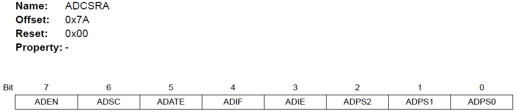
Bit 7 – ADEN: ADC Enable
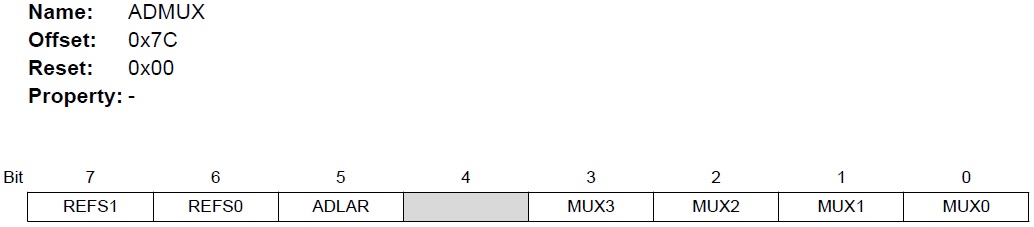
Bits 3:0—MUXn: Analog Channel Selection[n=3:0]
The value of these bits selects which analog inputs are connected to the ADC as the following table.
| MUX[3:0] | Single ended input |
|---|---|
| 0000 | ADC0 |
| 0001 | ADC1 |
| 0010 | ADC2 |
| 0011 | ADC3 |
| 0100 | ADC4 |
| 0101 | ADC5 |
| 0110 | ADC6 |
| 0111 | ADC7 |
| 1000 | Temperature sensor |
| 1001 | Reserved |
| 1010 | Reserved |
| 1011 | Reserved |
| 1100 | Reserved |
| 1101 | Reserved |
| 1110 | 1.1V (VBG) |
| 1111 | 0V (GND) |