
42.16 Watchdog Timer Graphs
00010 (4 ms))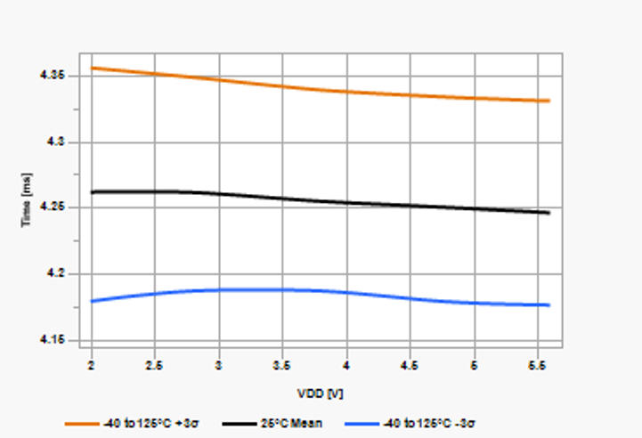
|
00010 (4 ms))
|
The online versions of the documents are provided as a courtesy. Verify all content and data in the device’s PDF documentation found on the device product page.