
1.2 Jumper Settings
The following figure shows the jumpers of the RT PolarFire Dev Kit.
Figure 1-3. Jumpers 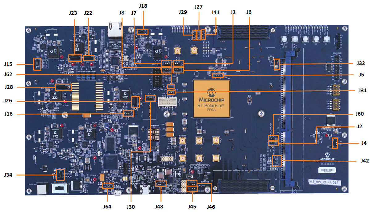
The following table lists the default jumper settings of the PolarFire Dev Kit.
| Jumper | Description | Pin | Default Settings |
|---|---|---|---|
| J60 | BANK 1 VREF for DIMM connector | — | Open |
| J2 | BANK 7 VREF for DIMM connector | — | Open |
| J41 | FMC1 connector HB BANK voltage | — | Open |
| J42 | FMC2 connector HB BANK voltage | — | Open |
| J27 | CLK_SEL1 pin for SerDes Mux | — | Open |
| J29 | CLK_SEL0 pin for SerDes Mux | — | Open |
| J31 | Mux select pin for RTPF silicon programming | — | Open |
| J62 | Mux select pin for SPI Flash or SPI DB | — | Open |
| J5 | XCVR_Vref pin | — | Open |
| J48 | Jumper to select VDD voltage to 1.0V and 1.05V | 2 and 3 | — |
| J45 | Jumper to select VDD_REG_SENSE- | 2 and 3 | — |
| J46 | Jumper to select VDD_REG_SENSE+ | 2 and 3 | — |
| J30 | Jumper to select VDDI1_7 voltage for MHP8565ASC RT regulator | 2 and 3 | — |
| J16 | VDDI1_7 voltage select jumper | 2 and 3 | — |
| J32 | VDDSPD voltage select jumper for DDR3 or DDR4 | 1 and 2 | — |
| J1 | LPRB_A or LPRB_B select jumper | 1 and 2 | — |
| J6 | Reserved pin for BANK3 pullup/pull down option | 1 and 2 | — |
| J7 | IO_CFG_INTF select jumper | 1 and 2 | — |
| J8 | SPI_Enable select jumper | 1 and 2 | — |
| J64 | USB3320_VBUS | 1 and 2 | — |
| J34 | 12PV enable select jumper | 1 and 2 | — |
| J28 | Jumper to select MHP50601A (RT regulator) or MIC2690 for VDD18 and VDDI0_6 | 1 and 2 | — |
| J26 | Jumper to select MHP8565ASC (RT regulator) or MIC2690 for VDD11_7 | 1 and 2 | — |
| J4 | Jumper to select VDDA voltage | 1 and 2 | — |
| J22 | Jumper to select VDDAUX2_5 voltage | 1 and 2 | — |
| J23 | Jumper to select VDDAUX4 voltage | 1 and 2 | — |
| J18 | Jumper to select VDDI2_5_Vadj_FMC1 voltage | 9 and 10 | — |
| J15 | Jumper to select VDDI4_Vadj_FMC2 voltage | 9 and 10 | — |