
10 Advanced Topics
Additional reading for advanced users.
10.1 Debugging a CLB Design
Designing an application that uses the CLB can be challenging. After configuration, the CLB logic operates independently of the CPU. Any internal states (BLE outputs) can be probed by routing those outputs to pins on the device, but this normally requires synthesizing the design again. This can have an unfortunate impact by altering the behaviour of the logic design you are trying to debug. To avoid intrusive debugging, some CLB implementations include one or more debug channels.
Using CLB debug channels
CLB debug channels provide one or more multiplexers that can connect to any of the BLE outputs. Crucially, these multiplexers are controlled by registers in the CLB peripheral that are not inside the bitstream. This means that the value can be modified without re-synthesizing the design.
- Allocate a PPS channel and pin to use for debugging, and set that PPS channel to the CLBDEBUG configuration at compile-time.
- Determine which BLE output is to be probed.
- Write the BLE number into the CLBDEBUG register in the CLB module. This can be done statically at compile time, dynamically from code, or during a debug session by changing the value in the I/O view.
Finding which BLE output to probe
When a CLB design is sent to the synthesis backend, the logic components sketched in the schematic editor are converted to Verilog constructs. Any Verilog included in the design is used as-is. After place-and-route, a graph is generated to represent the actual use of the CLB resources and is shown in the output section of the CLB Synthesizer GUI. This graph can show which BLE output performs which logic operation and can help in selecting which BLE output to probe. For more information on the graph output, see Synthesis Outputs.
The debug channels can probe the BLE output with or without the flip-flop, depending on how that BLE is configured.
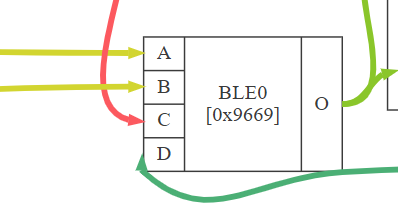
In this example, the output from BLE0 is not exposed via the flip-flop.
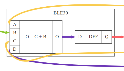
In this example, the output from BLE30 goes through the flip-flop (DFF). It is not possible to probe the raw LUT output without altering the logic design.
10.2 Clocking the Configurable Logic Block
How the CLB relates to clocks.
The CLB peripheral receives clock input from the source specified in the CLK field in the CLBCLK register, written from the CPU. Consult the data sheet for available clock sources.
The CLB also includes a clock divider, which must be configured along with the logic design and incorporated into the bit stream. The clock source can be divided by 1, 2, 4, 8, 16, 32, 64 or 128.
The CLB clock is distributed to all BLE flip-flops, so the logic design runs off the same clock. Although logic design schematics can include various flip-flop types, it is impossible to connect or configure an individual clock source.
10.3 Timing Report
Maximum Clock Calculation
The maximum operating frequency is derived by examining the post–place-and-route timing graph to determine the critical path(s) and using the established timing parameters of the CLB architecture to estimate the safe clock limit. At each clock transition, a signal launched from a synchronous source—typically a BLE flip-flop output—must propagate to the destination synchronous element before the subsequent clock transition. If the clock is too fast for this propagation to complete, setup timing violations may occur, resulting in unstable or incorrect system behavior.
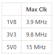
Example of a maximum clock frequency calculation.
Timing Report Maturity
| Maturity | Description |
|---|---|
| Provisional | The data in a provisional report is derived solely from simulations and has not been verified or adjusted in any way. |
| Preliminary | The data in a preliminary report is derived from simulations and is verified and/or adjusted using test results from a limited set of devices over restricted temperature and voltage ranges. |
| Final | A final report will not include a “provisional” or “preliminary” warning. Its data has been verified and/or adjusted using measurements from multiple devices tested across the full temperature and voltage range. However, the information is still subject to change and should be used for indication only. |
Graph Outputs and Highlighting
A number of graphs appear in the output section of the left-hand panel after synthesis and place-and-route is complete. These graphs can help visualize the resource usage of the CLB.
When viewing the graphical output after synthesis in the CLB Synthesizer toolchain, highlighting can help to identify various paths in the graph.
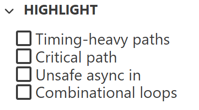
| Highlight | Description |
|---|---|
| Timing-heavy paths | Highlights all paths that may have a significant impact on the maximum clock frequency |
| Critical path | Highlights the path with the longest propagation delay. This path is used to determine the maximum clock frequency reported in the Max Clk table. |
| Unsafe async in | Highlights asynchronous inputs to the CLB up to the point where they become synchronised to the CLB clock, typically at the first flip-flop |
| Combinational loops | Highlights loops where logic outputs feed back as inputs without passing through a flip-flop |
Combinational Loops
A combinational loop occurs when the output of combinational logic feeds back into its own input path without being registered by a flip‑flop. Such loops are inherently risky because they can lead to metastability, oscillations, or other unpredictable and undesirable behavior in the design.
The CLB Synthesizer does allow combinational loops, and they can be implemented within the CLB. However, they should be used with great caution. The stability of a combinational loop depends on many factors—some of which are unknown to the CLB Synthesizer. As a result, if a combinational loop is detected, the timing report cannot determine a safe maximum CLB clock frequency.
Asynchronous Paths
An asynchronous path refers to a signal that is not synchronized to the CLB clock and may change value at any time. When such a signal is connected to the input of a synchronous element - typically a flip-flop - it becomes susceptible to metastability. Metastability can occur when the signal transitions too close to the clock edge of the receiving element, potentially resulting in unpredictable behaviour, instability, or even oscillation.
The Asynchronous paths into synchronous logic section of the timing report identifies the locations of asynchronous signals within the design and shows where they interface with synchronous logic.
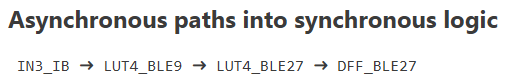
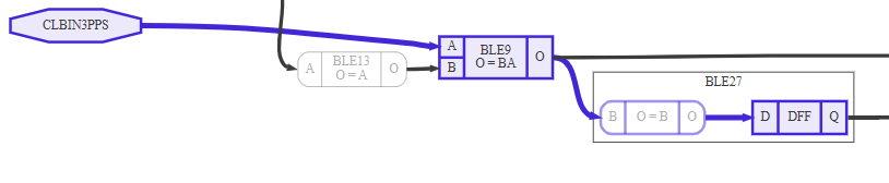
In this example, IN3 is an asynchronous input that is connected to BLE9 with its flip-flop bypassed. The resulting combinational output is routed to BLE27, whose flip-flop is enabled and serves as the first synchronous element encountered by this signal.
Critical Paths for Synchronous Logic
The Critical sync-sync paths section of the timing report identifies the critical timing paths for the logic design at the evaluated voltage levels. These paths form the input data used to compute the values reported in the Maximum Clock table.
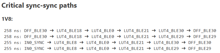
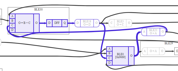
In this example, the critical path is highlighted as a loop from BLE30 through BLE18, BLE0, BLE21, and back to BLE30.
Timing Tips and Tricks
The timing of digital signals can be affected by numerous factors, including those originating within the CLB itself, those elsewhere in the device, and those external to the device.
| Area | Behaviour | Mitigation |
|---|---|---|
| CLB | A long critical path results in a substantial accumulated propagation delay, which may be further increased when BLEs are repurposed as routing resources rather than being used solely for logic implementation | Try to refactor the design to shorten timing-critical paths. Where feasible, insert additional flip-flops to break up long combinational chains and reduce the overall propagation delay. |
| A signal within the CLB that drives a large fanout—feeding multiple BLE inputs—can experience increased propagation delay compared to a single point-to-point connection | Try to refactor the design | |
| Device | The drive strength of the device’s I/O pins can influence overall CLB performance. Note that the timing report reflects only delays within the CLB and does not account for any external I/O-related timing. | Measure the behavior on actual hardware and adjust the design parameters accordingly |
| Board | PCB layout can influence the propagation characteristics of signals traveling from the device to external components | Adding a flip-flop to the output signal can improve performance |
The input impedance of external components driven by signals originating in the CLB can also influence overall timing performance |
10.4 Preferences
The preferences panel is accessed via the main drawer menu.
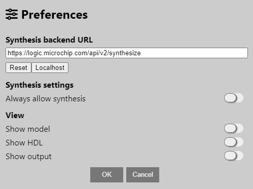
| Option | Description |
|---|---|
| Synthesis backend URL | The synthesis server URL must not be changed unless instructed to by Microchip support engineer |
| Always allow synthesis | Used to bypass Design checker errors by graying out the Synthesize button |
| Show model | The right-hand pane will show the “GUI model” of the current design—this is for internal debugging of the GUI |
| Show HDL | The right-hand pane will show the intermediate HDL of the current design. This content will be sent to the backend for synthesis, for internal debugging of the interface between the GUI and backend |
| Show output | The right-hand pane will show output from the synthesis engine—this is for internal debugging of the backend logic-synthesis engine |
10.5 Making Use of the Output ZIP
How to use the output.
The synthesis process always returns a ZIP file with outputs.
The ZIP file is intended for the CLB Synthesizer Web version's users who want to convert a logic design into a bit stream.
- The resultant bit stream
- A basic CLB driver for configuring the peripheral
- Build artifacts
Refer to the readme inside the ZIP for further details.
10.6 Description of Output Files
After synthesis, a ZIP file containing many build artifacts can be downloaded.
- Root folder: Outputs for use in bare metal projects
- Build folder: Debug artifacts from the build process
- Input folder: Inputs passed into the server for processing
| Filename | Description |
|---|---|
readme.txt | Instructions for bare-metal users |
clb1.c; clb1.h | Driver for configuring and enabling the CLB |
clb1_defs.h | Header file defining useful constants for the CLB |
clb1_output_mappings.h | Header file defining output mappings from the CLB to peripherals |
bitstream.S | Bitstream in assembler format for embedding into a bare-metal project |
pre-routing.svg | Diagrammatic representation output from Yosys (generic) |
routed.svg | Diagrammatic representation post-routing |
timing.md | Timing report |
build/bitstream.json | Bitstream words in JSON format |
build/out.fasm | Output from the FASM stage |
build/out.net | Pre-routing packed netlist in XML format |
build/out.net.post_routing | Post-routing packed netlist in XML format |
build/out.netlist | Binary form of the netlist |
build/out.phys | Binary form of the physical netlist |
build/out.place | Placer output report |
build/out.route | Router output report |
build/packaging_pin_util.rpt | Packing pin usage report |
build/pre-routing.v | Verilog netlist output from Yosys (before place and route) |
build/routed.v | BELs format netlist post-routing |
build/stderr.txt | Backend stderr log |
build/stdout.txt | Backend stdout log |
build/vpr_stdout.log | Place-and-route output |
build/yosys.log | Log from the Yosys synthesis stage |
build/synth.json | JSON-formatted netlist output from Yosys |
input/*.v | Verilog representation of the input design |
input/*.xdc | Mappings to physical pins |
input/project.json | Top-level description of the design |
input/stats.json | Statistical summary of the design |
input/*.clb | Save-file for the design |
10.7 Synthesis and Place-and-Route Process
What happens behind the scenes?
Once an application has been captured in the CLB Synthesizer GUI, it needs to be converted into a configuration bit stream, which can be loaded into the CLB module. This process is known as “synthesis”, although it also includes place and route steps and is done by Microchip’s online web service.
It is unnecessary for the user to understand how this process works—a brief summary is given here for advanced or curious users.
How It Works
- The CLB application schematic drawings are converted to equivalent Verilog descriptions and sent to the backend for processing.
- The first stage in the backend process is logic synthesis. Logic synthesis is a process to convert the Verilog textual representation of a logic design into a netlist, which describes the hardware in equivalent logic gates and wires. Logic synthesis is done using Yosys Open SYnthesis Suite, which is equipped with a plug-in describing the actual structure of the logic elements in the CLB module. The output of the synthesis stage is a Verilog netlist.
- The next stage is Place-and-Route (PnR). During this stage, the netlist elements are mapped into physical locations in the CLB array (placement), and interconnects are made between them (routing), which is a complex and iterative process and is not ensured to achieve an outcome (e.g., if exceeding space or routing constraints). PnR is done using the VPR provided by Verilog to Routing (VTR), which is equipped with a plug-in that describes the available interconnects within the CLB module. The output of the PnR stage is a FASM file, which specifies the CLB configuration content in a generic, plain-text format.
- The final stage is bit stream generation. The bit stream generator parses the FASM file and converts the configuration of generic configurable logic resources into bit patterns in a bit stream according to the actual CLB bit stream implementation. The bit stream generator is a script specific to the Microchip CLB implementation. The output of the bit stream generator is a sequence of bits to be loaded into the CLB during configuration, which embeds as a sequence of data words (DW) stored as constants in Flash by the compiler during application building.