
5 Interacting With Pins, Peripherals and the CPU
How to connect the CLB, CPU, pins and other peripheral modules.
5.1 Interacting With Pins
The CLB does not have direct access to input or output pins on the MCU. All interaction between the CLB and pins is done using the PPS module.
When using the CLB Synthesizer, the I/O Port selector can be set to one of the PPS channels, but the CLB Synthesizer does not configure PPS in any way.
5.1.1 Input From Pins to the CLB
Using the value of a pin in the CLB.
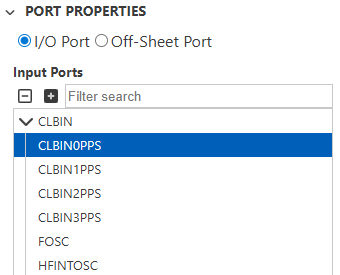
A number of PPS input channels can be used in the CLB and are made available in the CLB Synthesizer through the Input Ports selector.
Input signals from PPS pass through the Input Synthronizers upon entering the CLB. For more information, see Input Synchronizers.
5.1.2 Output to Pins From the CLB
Driving a pin from the CLB.
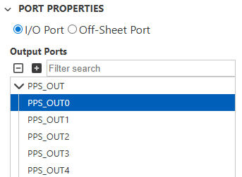
The CLB can use a number of PPS output channels. They are made available in the CLB Synthesizer through the Output Ports selector.
5.1.3 Controlling the I/O Pin Data Direction
Enable and disable the pin output driver to drive a tri-state bus.
Logic signals within the CLB peripheral can be used to control the pin output drivers on the microcontroller, enabling the implementation of features such as tri-state bus driver circuitry.
The control signals must be routed from the CLB and, in some cases, may pass through additional multiplexers before reaching the I/O pin on the device. This routing architecture can differ between device families, so it is important to thoroughly understand which elements are managed by the CLB Synthesizer.
The CLB Synthesizer toolchain is responsible only for configuration settings contained within the bitstream. Similar to indirect I/O ports, as described in Using Direct and Indirect I/O Ports, data direction ports can be included in the I/O port selection panel. This selection configures the relevant bits in the CLB bitstream only and does not fully configure the routing to the data direction control register.
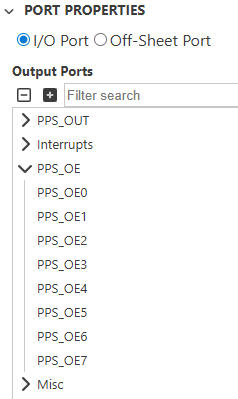
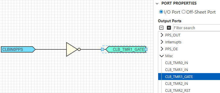
Below is an example of how to select the Output Enable port on a PIC16F13145 family device.
When using the CLB Synthesizer within MCC, the graphical user interface allows you to configure the appropriate pin direction register. For users of the web version of the CLB Synthesizer toolchain, the clb1_output_mappings.h file within the downloaded ZIP provides information on additional configuration steps required to complete the routing from the CLB to the pin controller. This ZIP file is available for download after synthesis.
5.2 Interacting With Peripherals
The interaction between CLB and other peripherals is achieved through input ports from these peripherals and output ports to these peripherals within a logical design framework. Consult the device data sheet for information on how these signals are used by the corresponding peripheral.
5.2.1 CLB Inputs from Other Peripherals
How to route signals from other peripheral modules to the CLB.
Signals from various peripherals within the microcontroller can be connected to the CLB as inputs. This is a two-stage process.
Step 1: Configure an Input to the CLB
In the CLB Synthesizer GUI, configure an input port by selecting the peripheral signal to use in the Port Properties panel.
Synthesize the logic design.
Step 2: Configure the Peripheral
The peripheral to which the CLB connects must be configured accordingly, which is peripheral-dependent. Consult the data sheet for more information.
MCC Users
After synthesis, the peripheral being used will be added to the MCC project automatically, but it must still be configured.
5.2.2 CLB Outputs to Other Peripherals
How to route signals from the CLB to other peripheral modules.
The CLB BLE outputs can be connected to various other peripherals, which is a two-stage process:
Step 1: Configure an Output From the CLB
In the CLB Synthesizer GUI, configure an output port by selecting the peripheral signal to route to in the Port Properties panel.
Synthesize the logic design.
Step 2: Configure the Peripheral to Accept the Signal From the CLB
The peripheral to which the CLB connects must be configured to receive the CLB input signal, which is peripheral-dependent. Consult the data sheet for more information.
MCC Users
After synthesis, the peripheral being used will be added to the MCC project automatically, but it must still be configured.
Web/Bare Metal Users
Users of the web version need to download the ZIP output from the synthesis process and
examine (or use directly) the contents of clb1_output_mappings.h file,
which provides values for use in the peripheral configuration register.
5.3 Using Direct and Indirect I/O Ports
When adding an I/O port to a logic design, the list of ports available in the Port Properties depends on the device in use. Some of these resources can be accessed directly from the CLB, while others must be used indirectly.
Devices using BLE outputs directly
In some device families, such as the PIC16F13145 family, output connections from the CLB to other peripherals' inputs are made by connecting directly to BLE outputs. The peripheral's input selector specifies an individual BLE number, or a range of BLEs numbers, the output of which can be used as input to that peripheral.
Devices with CLB Output Trigger Channels
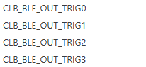
In some device families, such as the PIC16F13275 family, connections from the CLB to other peripherals are made using CLB output trigger channels. These are limited resources available for making such connections within the microcontroller. A peripheral that can accept a trigger from the CLB has one or more CLB_BLE_OUT_TRIG[n] selections in its input selection register.
The CLB Synthesizer includes both directly accessible resources and indirectly accessible resources in the Port Properties view. Indirectly accessible resources are shown with tag icons.
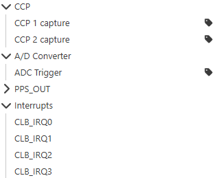
CCP 1, CCP 2, and the ADC Trigger are indirect peripheral connections that need to use a trigger channel, while the CLB_IRQn connections can be used directly from the CLB.
The trigger channels themselves are directly accessible resources that are used to access the indirectly accessible resources.
// Device signal TMR3CLK was mapped to clb port CLB_BLE_OUT_TRIG05.4 Input Synchronizers
Making use of synchronizers on input signals.
The CLB peripheral includes 16 input sources, which connect the CLB to external signals and the 32 CLBSWIN signals for interacting with the CPU. The 16 input sources include modifiers that can condition the incoming signal before entering the BLE matrix.
Input synchronizer options are selected on the right-side properties panel below the input port source selection box.
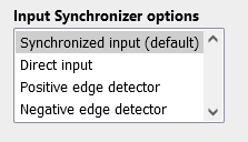
The following table shows the available input synchronizer options:
| Option | Description |
|---|---|
| Synchronized input | The input signal will be synchronized to the CLB clock, which is the default and safest option when unsure |
| Direct input | Synchronization is bypassed, and the input signal is connected directly to the BLE input. Use it carefully, as this can cause metastability in sequential logic designs. |
| Positive edge detector | A rising edge on the input signal will generate a pulse synchronized to the CLB clock |
| Negative edge detector | A falling edge on the input signal will generate a pulse synchronized to the CLB clock |
- The CLBSWIN signals cannot pass through the input synchronizers. These inputs from the CPU are synchronous by design.
- The input synchronizer is selected in hardware with three configuration bits, but not all eight possible permutations are made available in the CLB Synthesizer.
5.5 Interacting With the CPU
Interaction between the CPU (running code) and the CLB using the CLBSWIN register.
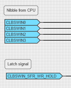
5.5.1 Using CLBSWIN
The CLB Software Input register (CLBSWIN) enables the MCU to communicate directly with the logic design in the CLB. So for example, this can be used to load a value into the CLB at run time.
To make use of the CLBSWIN register within a logic design, simply use the individual CLBSWINn bits as input ports.
If a logic design needs to trigger an action when a new value is written to CLBSWIN, then the CLBSWIN_SFR_WR_HOLD input signal can be used. This signal is asserted when the CPU writes a new value to CLBSWIN and that value have been latched into the CLB.
- The CLBSWIN register cannot be used via the input synchronizers.
- The CLBSWIN_SFR_WR_HOLD signal is asserted only when the lower eight bits of CLBSWIN are written (CLBSWINL), so the byte must be written after writing the upper bytes in CLBSWIN.
5.5.2 Using CLBSWOUT
In many applications, it is useful for the CPU to read data from the CLB. This is done by reading the CLBSWOUT register(s).
The CLBSWOUT[0..n] signals are included in the CLB Synthesizer toolchain as regular output signals. Each individual bit of the register can be driven by the CLB and read by the CPU, where it can be used as either an n-bit value or as individual bits according to needs of the application.
CLBSWOUT in the PIC16F13145 family of devices
When using these devices, the output of each BLE in the CLB is routed to the 32-bit CLBSWOUT register, which enables the CPU to read the current state of the CLB. It is not possible to specify in the CLB Synthesizer that certain signals must be locked to specific BLE outputs - it is up to the place-and-route algorithm to allocate these resources. However, it is possible to determine after synthesis which signals are actually placed on which BLE outputs by examining the output graphs. For more information, see Synthesis Outputs.
5.6 Interrupting the CPU
A CLB logic design can interrupt the MCU using one of the interrupt output signals from the CLB. In the CLB Synthesizer toolchain, use a regular output port and select one of the available signals from the Interrupts section in the Port Properties view.
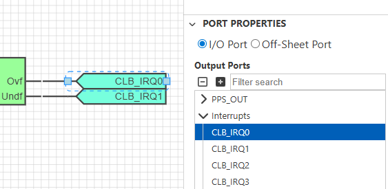
Interrupt signal names depend on the device. See the device data sheet for more information on how interrupts are handled on that particular device.
An interrupt signal from the CLB to the CPU must be treated with caution. Each pulse of that signal can potentially stall the application while the interrupt is serviced, which could lead to CPU starvation.