
3 The Synthesis Process, Status and Outputs
Understanding the synthesis process and interpreting its results.
3.1 Status of the Synthesis Process
Understanding the synthesis status indicator.
A synthesis process converts a logic design into bit stream form, which can be loaded into the CLB. Clicking the Synthesize button will trigger this.
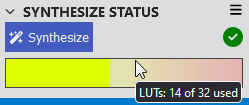
The status indicator and the resource view indicate the outcome of the synthesis process.
Successful Synthesis
A green indicator shows when the synthesis succeeds, and the resource view is updated.
Failed Synthesis
A red indicator shows when synthesis has failed.
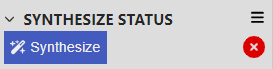
The nature of the failure can be determined by:
- Checking the Design checker or Notifications panels for warnings about unconnected pins
- Checking the Synthesis panel for output from the backend synthesis process
- Downloading the ZIP and checking the backend log output, which must also be included when consulting the Microchip support channels
3.2 Synthesis Outputs
Additional outputs other than the bit stream.
The primary output of the Synthesis process is the bit stream. However, there are additional outputs in the ZIP file which may be useful.
Two diagrams are produced during synthesis and displayed in the output panel on the left sidebar.
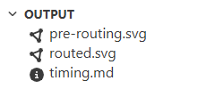
The examples here are the result of synthesizing this design:
pre-routing.svg
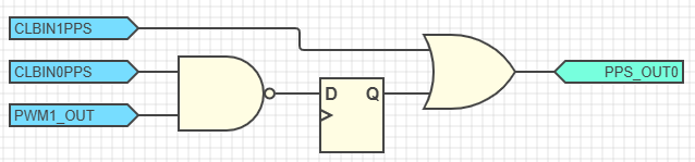
This diagram shows a presentation of your logic design after YoSYS has processed it but before mapping it into CLB-specific resources.
- CLBIN0PPS and PWM1_OUT are connected to inputs A and B of a LUT with the logic function O = ¬B + ¬A
- The output of the LUT is routed through the flip-flop (DFF)
- This DFF output is connected to a LUT along with CLBIN1PPS, with the logic function O = B+A
- The output of this LUT is connected to PPS_OUT0

routed.svg
This diagram shows a representation of your logic as it will be implemented on the actual CLB hardware using its available resources.
- CLBIN1PPS uses input IN0. Hover over this node to see its synchronizer setting.
- PWM1_OUT uses input IN1. Hover over this node to see its synchronizer setting.
- CLBIN0PPS uses input IN2. Hover over this node to see its synchronizer setting.
- CLBIN0PPS uses BLE29 as a routing node to reach BLE30. It is shown in grey with the function O = A.
- BLE6 implements the logic function O = A + D
- The output of BLE6 uses BLE3 as a routing node to reach the output PPS_OUT0. It is shown in grey with the function O = A.
- BLE30 implements the logic function O = ¬D + ¬A and has its flip-flop (DFF) enabled

By counting the number of BLEs that the logic signals pass through between synchronization points (flip-flops) it is possible to estimate a safe operating frequency for the logic design in conjunction with timing information in the device data sheet. For more information, see Timing Report.
3.3 Resource Usage Debugging
- Try to use alternative outputs (e.g., change IRQ0 to IRQ1)
- Try to remove some logic functionality
- Check that there are no unused modules included in the documents
- Check that there are no logic functions with predetermined outputs (e.g., a constant zero as an input to an AND gate)
Include the ZIP file returned from the failing synthesis process when contacting Microchip support.