
4.2.1 JTAG
The JTAG interface consists of a 4-wire Test Access Port (TAP) controller that is compliant with the IEEE® 1149.1 standard. The IEEE standard was developed to provide an industry-standard way to efficiently test circuit board connectivity (Boundary Scan). Atmel AVR devices have extended this functionality to include full Programming and On-Chip Debugging support.
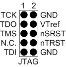
When designing an application PCB which includes an AVR with the JTAG interface, it is recommended to use the pinout as shown in Figure 4-2. The JTAGICE mkII 100-mil probe connectors support this pinout.
| Name | Pin | Description |
|---|---|---|
| TCK | 1 | Test Clock (clock signal from the JTAGICE mkII into the target device) |
| TMS | 5 | Test Mode Select (control signal from the JTAGICE mkII into the target device) |
| TDI | 9 | Test Data In (data transmitted from the JTAGICE mkII into the target device) |
| TDO | 3 | Test Data Out (data transmitted from the target device into the JTAGICE mkII) |
| nTRST | 8 | Test Reset (optional, only on some AVR devices). Used to reset the JTAG TAP controller. |
| nSRST | 6 | Source Reset (optional). Used to reset the target device. Connecting this pin is recommended since it allows the JTAGICE mkII to hold the target device in a reset state, which can be essential to debugging in certain scenarios - for example if the JTD bit is set by the application firmware, disabling the JTAG interface. The nSRST pin has an internal pullup resistor in the JTAGICE mkII. |
| VTref | 4 | Target voltage reference. The JTAGICE mkII samples the target voltage on this pin in order to power the level converters correctly. The JTAGICE mkII draws less than 1mA from this pin. |
| GND | 2, 10 | Ground. Both must be connected to ensure that the JTAGICE mkII and the target device share the same ground reference |
Tip: remember to include a decoupling capacitor between pin 4 and GND.
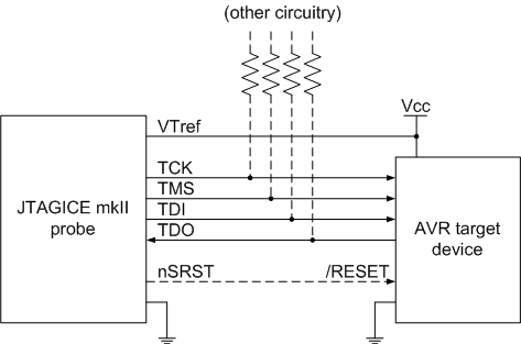
When external circuitry shares the JTAG debug lines on the target application, series resistors should be used to avoid driver contention, as shown in Figure 4-1. The value of the resistors should be chosen so that the external circuitry and the AVR do not exceed their maximum ratings (i.e. sink or source too much current). 1kΩ is a commonly used value.
It is recommended to disconnect any analog filters on these lines (which should be on the 'outside' of the resistors) during a JTAG session, since these elements are discharged by the JTAG signals, possibly causing false logic levels influenced by the residual voltage in the capacitor. If the filters cannot be disconnected, it is then recommended to apply target VCC directly to the capacitor during a session to hold the voltage stable. Be sure to use a large enough resistor between the capacitor and the JTAG line when doing this!
The JTAG interface allows for several devices to be connected to a single interface in a daisy-chain configuration. The target devices must all be powered by the same supply voltage, share a common ground node, and must be connected as shown in Figure 4-3.
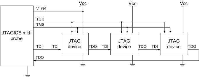
When connecting devices in a daisy-chain, the following points must be considered:
-
All devices must share a common ground, connected to GND on the JTAGICE mkII probe
-
All devices must be operating on the same target voltage level. VTref on the JTAGICE mkII probe must be connected only to VCC on the first device in the chain.
-
TMS and TCK are connected in parallel; TDI and TDO are connected in a serial chain.
-
NSRST on the JTAGICE mkII probe must be connected to RESET on the devices if any one of the devices in the chain disables its JTAG port
-
"Devices before" refers to the number of JTAG devices that the TDI signal has to pass through in the daisy chain before reaching the target device. Similarly "devices after" is the number of devices that the signal has to pass through after the target device before reaching the JTAGICE mkII TDO pin.
-
"Instruction bits before" and "after" refers to the sum total of all JTAG devices' instruction register lengths which are connected before and after the target device in the daisy chain
-
The total IR length (instruction bits before + instruction bits after) is limited to a maximum of 32 bits
Daisy chaining example: TDI -> ATmega1280 -> ATxmega128A1 -> ATUC3A0512 -> TDO
In order to connect to the Atmel AVR XMEGA device, the daisy chain settings are:
Devices before: 1
Devices after: 1
Instruction bits before: 4 (AVR devices have four IR bits)
Instruction bits before: 5 (Atmel AVR 32-bit microcontrollers have five IR bits)