1.1 PL360G55Cx-EK + ATREB215-XPRO-A
This supported platform is composed of two different evaluation boards:
- The first board, a PL360G55Cx-EK (PL360G55CF-EK for CENELEC-A or FCC working bands or a PL360G55CB-EK for CENELEC-B working band), includes the host controller, a SAMG55J19, to run the application and the upper layers of the stack, and the PLC device, PL360, to run the PHY and MAC-RT layers for PLC communications.
- The second board is an ATREB215-XPRO-A with the AT86RF215 to run the PHY layer for the RF communications. The RF module is configured to run on the sub-GHz band.
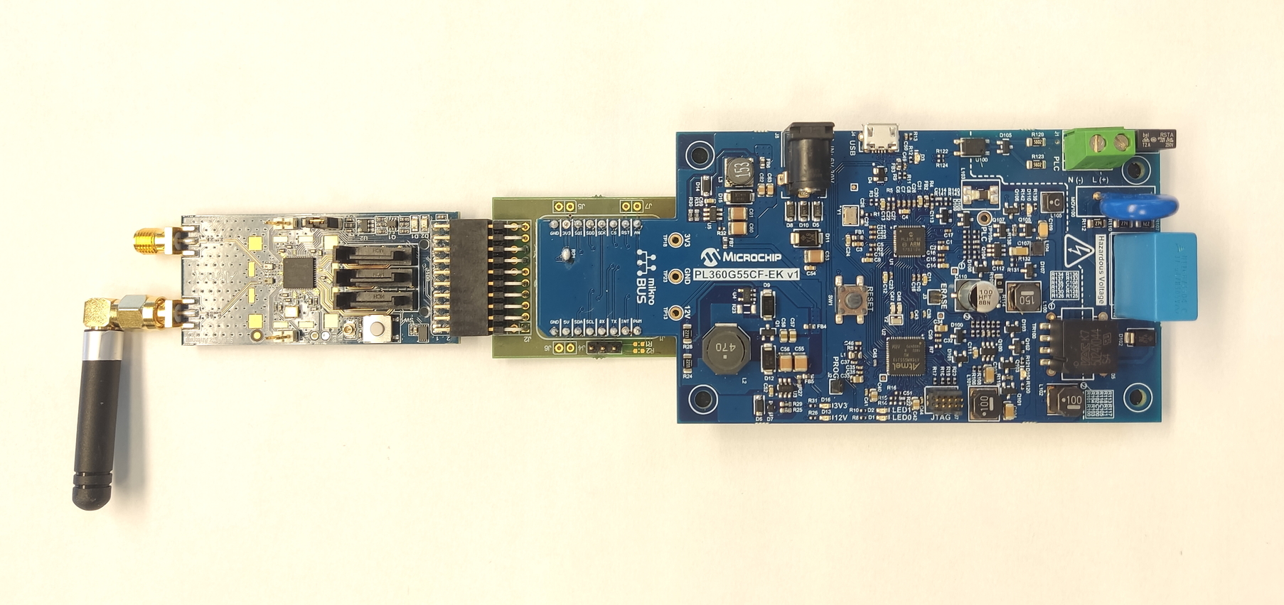
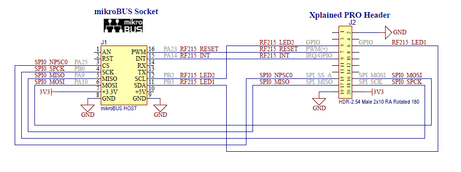
The PL360G55Cx-EK uses the USB connector (J4) to communicate with a PC via console and the MikroBUS to communicate with the ATREB215-XPRO-A. The lines used in the connection between both boards are described in the following table and figure:
| Description | mikroBUS Socket (PL360G55Cx-EK) | Xpained PRO Header (ATREB215-XPRO-A) |
|---|---|---|
| Power | 7 (+3.3V) | 20 (3V3) |
| GND | 8 (GND) | 2 (GND) |
| 9 (GDN) | 19 (GND) | |
| SPI | 3 (CS) | 15 (SPI_SS_A) |
| 4 (SCK) | 18 (SPI_SCK) | |
| 5 (MISO) | 17 (SPI_MISO) | |
| 6 (MOSI) | 16 ( SPI_MOSI) | |
| RF215 Reset | 16 (PWM) | 7 (PWM+) |
| RF215 Interruption | 15 (INT) | 9 (IRQ/GPIO) |
| LED1 | 11 (SDA) | 6 (GPIO2) |
| LED2 | 12 (SCL) | 5 (GPIO1) |
Important: To power up the
ATREB215-XPRO-A board from a PL360G55Cx-EK board, it is required to mount a 0-Ohm
resistor in the footprint close to the mikroBus pin of +3.3V (R21 in PL360G55CF-EK or
R22 in PL360G55CB-EK).
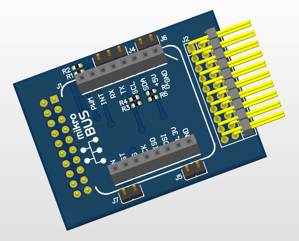
The design files of a customized adapter from mikroBus to Xplained PRO to connect PL360G55Cx-EK and ATREB215-XPRO-A boards is available from the Microchip website.