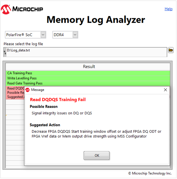
Signal integrity issues on DQ or DQS lines. When check 1 of the Read DQDQS training fails, a
dialog box appears as shown in the following figure.Figure 5-8. Read DQDQS
Training
Workaround
Configure any one of the following parameters to a different value using the MSS Configurator
when check 1 of the Read DQDQS training fails:
Decrease the FPGA DQDQS
start training window offset
FPGA DQ ODT
FPGA Vref Data
Memory Output Drive
Strength
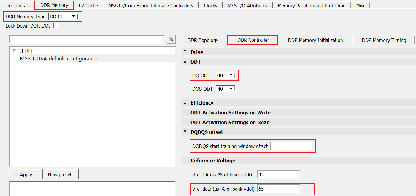
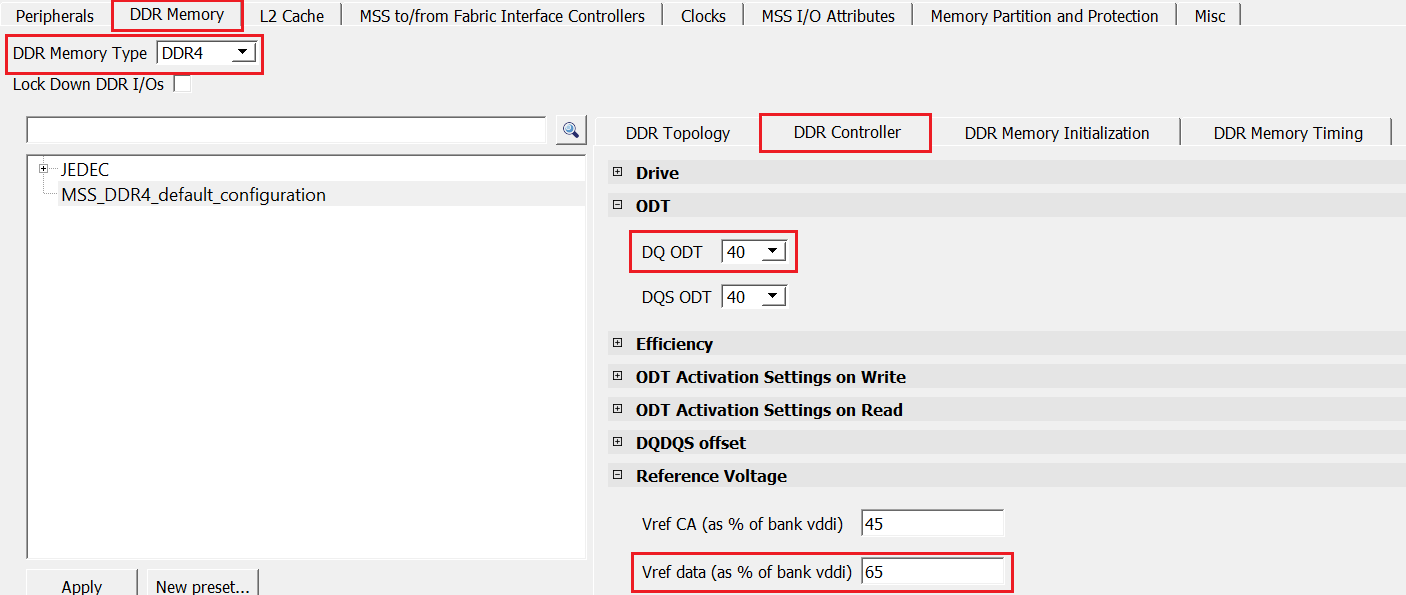
The following figure shows the configuration of DQ ODT, DQDQS start
training window offset, or Vref data in the DDR
Controller tab.
Figure 5-9. Configuring DQ ODT,
DQDQS Start Training Window Offset or Vref Data—DDR Controller
Tab
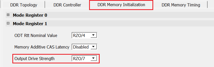
The following figure shows the configuration of output drive strength
in the DDR Memory Initialization tab.
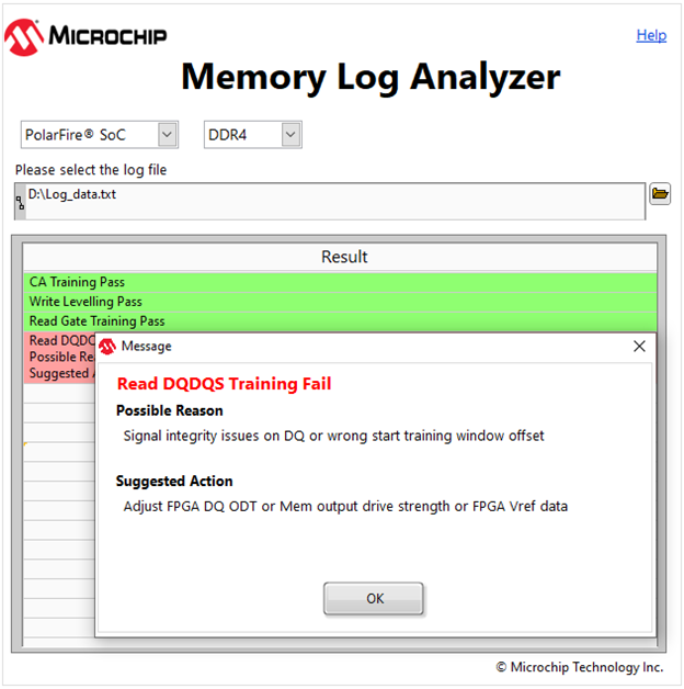
Signal integrity issues on DQ or wrong start training window offset. When check 2 of the Read
DQDQS training fails, a dialog box appears as shown in the following figure.Figure 5-11. Read DQDQS
Training
Workaround
Configure any one of the following parameters to a different value using the MSS Configurator
when check 2 of the Read DQDQS training fails:
FPGA DQ ODT
FPGA Vref Data
Memory Output Drive
Strength
The following figure shows the configuration of DQ ODT or Vref data in the
DDR Controller tab.Figure 5-12. Configuring DQ ODT or
Vref Data—DDR Controller TabThe following figure shows the configuration of output drive strength in
the DDR Memory Initialization tab.Figure 5-13. Configuring Output
Drive Strength—DDR Memory Initialization Tab
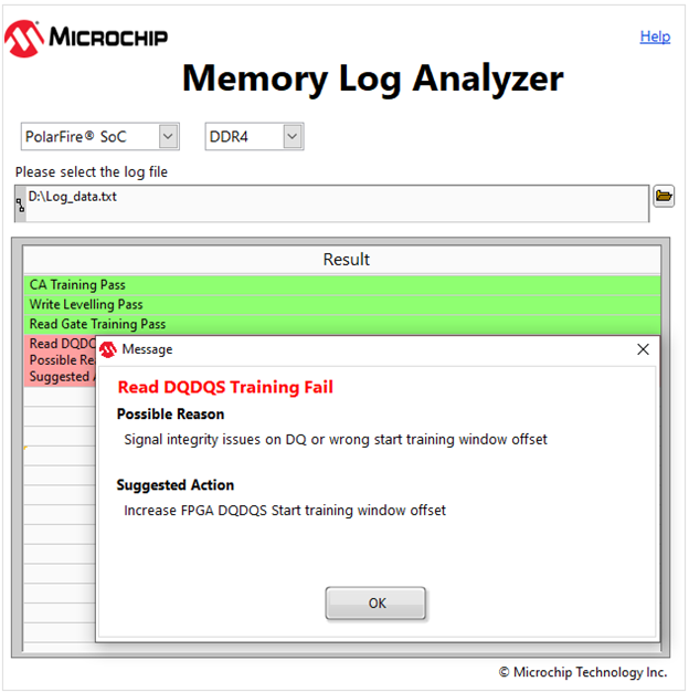
Signal integrity issues on DQ or wrong start training window offset. When check 3 of the Read
DQDQS training fails, a dialog box appears as shown in the following figure.Figure 5-14. Read DQDQS
Training
Workaround
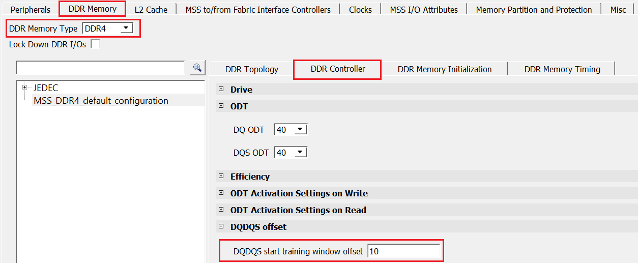
Increase the FPGA DQDQS start training window offset value when check 3 of the Read DQDQS
training fails, see the following figures.Figure 5-15. Configuring DQDQS
Start Training Window Offset—DDR Controller Tab