Alternative Methods for Voltage Conversion
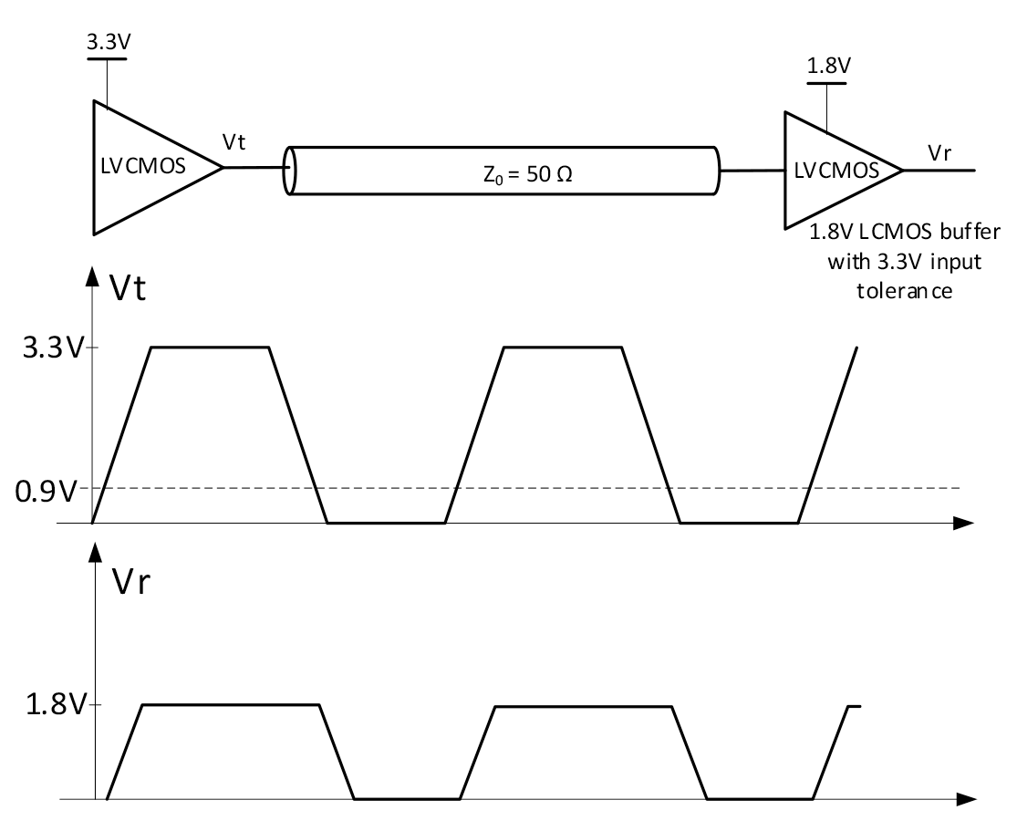
The first method to consider is going from high to low voltage (for example, from 3.3V LVCMOS to 1.8 LVCMOS). Users can achieve this by using a receiving component (1.8 LVCMOS buffer) with inputs that can tolerate 3.3V, as shown in the following figure. Even when using a clock buffer with the required input voltage tolerance, the output clock duty-cycle will increase because the sampling level is not at 50% of the input signal. In the case of a 1.8V voltage buffer, the threshold level is 0.9V and one can see that the output clock duty-cycle will be significantly higher than 50%. The duty-cycle would be even more distorted if the receiving component is a 1.5V or 1.2V LVCMOS buffer. Additionally, while the typical threshold of LVCMOS devices is 0.5VDD, over the process and temperature variations of most data sheet specifications, the typical threshold is a range from 0.3VDD to 0.7VDD. This further increases duty-cycle distortion.
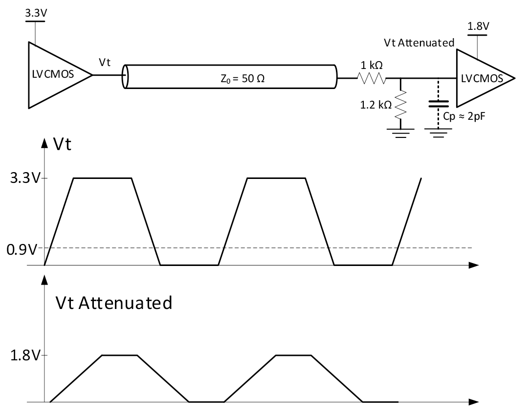
Another method for going from higher to lower voltage levels is to use a resistive voltage divider to reduce the signal level from 3.3V to 1.8V or lower, as shown in the figure above. The problem with this method is signal integrity because resistors in voltage dividers need to be much higher than 50Ω. This is because LVCMOS outputs typically cannot drive the high current required by a 50Ω load. Resistors in this case need to be a few hundred ohms to kilo-ohms. For example, the conversion could be achieved with a 1kΩ resistor plus a 1.2kΩ resistive divider at the receiving end. This method does not work for higher frequencies because of the low-pass filtering effect on the clock from a series resistor in the divider and the parasitic capacitance of the receiving device, which reduces rise and fall times. For a typical input capacitive parasitic load of 2pF, the RC constant is 2ns. Rise/fall times are roughly 2.2RC constant (for first order filter). So even if the driver has very fast rise/fall times, the receiving device will see very slow rise/fall times of 4.4ns. This, in turn, results in an additive jitter increase because of the amplitude noise to phase noise conversion, which is proportional with clock rise/fall times.
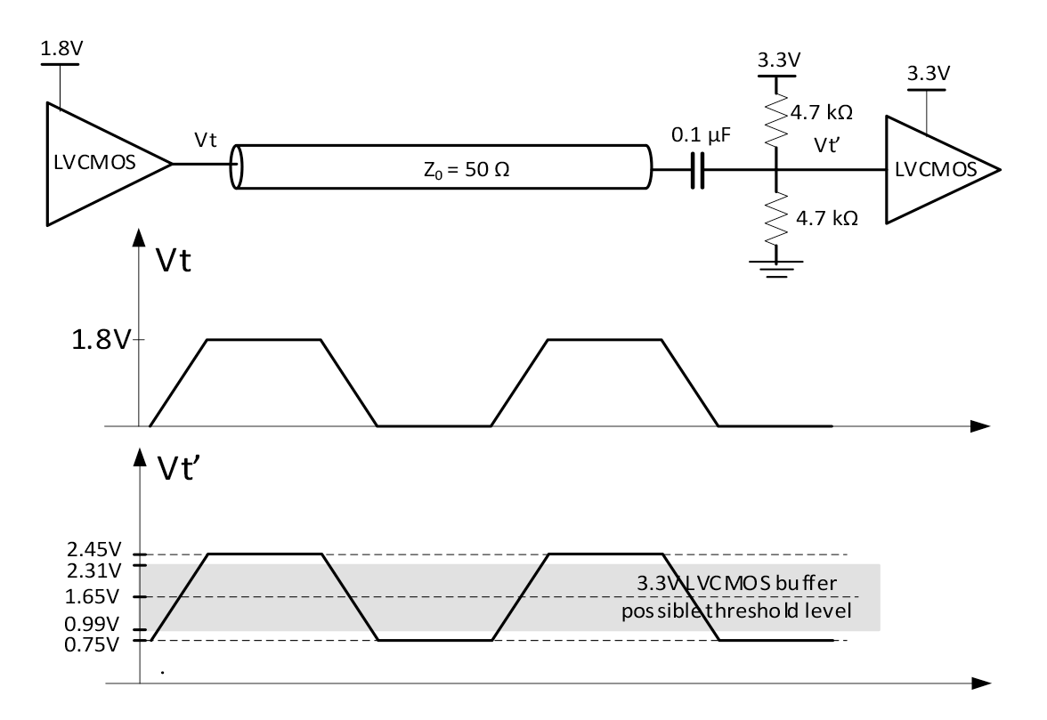
When going from an LVCMOS buffer with low VDD to an LVCMOS buffer with high VDD, users need to raise the transmitting clock DC level such that transitions are toggling around the receiving device threshold level. This can be achieved with AC coupling and biasing, as shown in the following figure. The problem with this method is that the threshold level of LVCMOS devices is not always at the VDD/2, but, with taking process and temperature into account, that threshold can vary between 0.3VDD and 0.7VDD. For a VDD of 3.3V, this means that the threshold range of a 3.3V LVCMOS buffer is between 0.99V and 2.31V. Clearly, this method cannot be used to convert from 1.2V to 3.3V. Even for 1.8V to 3.3V conversions, this method will give unpredictable duty-cycle at the output due to threshold variations. In addition, one can see that the margin is very small and if one factors in the tolerance of input and output buffer devices (typically ±5%), the device quickly runs out of any available margin.