
8.6.3.2 Timing in TRANSMITTING and NORMAL (Receive) States
This section documents timing specifications for TX, RX, ED and the differential pair TRXN/TRXP when in TRANSMITTING or NORMAL states.
TX, RX, and TRXN/TRXP Signals when Transmitting or Receiving
This section documents the timing of TX, RX and the differential pair TRXN/TRXP when no state transitions have recently occurred.
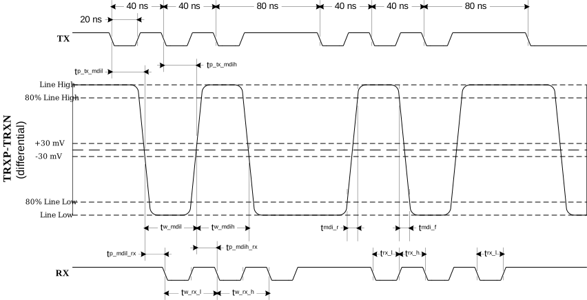
| Parameter | Symbol | Min | Typ | Max | Units | Additional Information | |
|---|---|---|---|---|---|---|---|
| TX and TRXP/N Characteristics (TRANSMITTING state only) | |||||||
| Propagation delay from falling edge of TX to rising edge on TRXP/N |
tp_tx_mdih | — | — | 50 | ns | Measured from falling edge crossing 50% level on TX to TRXP/N rising voltage crossing +30mV | |
| Propagation delay from falling edge of TX to falling edge on TRXP/N |
tp_tx_mdil | — | — | 50 | ns | Measured from falling edge crossing 50% level on TX to TRXP/N falling voltage crossing -30mV | |
| TRXP/N negative pulse width |
tw_mdil | 36 | — | 44 | ns |
Measured from TRXP/N falling voltage crossing of -30 mV to TRXP/N rising voltage crossing of +30 mV during a DME 1 symbol | |
| TRXP/N positive pulse width |
tw_mdih | 36 | — | 44 | ns |
Measured from TRXP/N rising voltage crossing of +30 mV to TRXP/N falling voltage crossing of -30 mV during a DME 1 symbol | |
| RX and TRXP/N Characteristics | |||||||
| Propagation delay from falling edge on TRXP/N to falling edge of RX |
tp_mdil_rx | — | — | 80 | ns |
Measured from a TRXP/N falling voltage crossing -30 mV to falling edge crossing 50% level on RX during a DME 1 signal | |
| Propagation delay from rising edge on TRXP/N to falling edge of RX |
tp_mdih_rx | — | — | 80 | ns |
Measured from a TRXP/N rising voltage crossing +30 mV to falling edge crossing 50% level on RX during a DME 1 signal | |
| RX negative pulse width |
trx_l | 12 | — | — | ns | Width of a low pulse on RX | |
| RX positive pulse width |
trx_h | 12 | — | — | ns | Width of a high pulse on RX during a DME 1 signal. | |
| TRXP/N to RX receive symmetry (low) | trx_sym_l | -4 | — | +4 | ns |
Difference between width of low half cycle of an input DME 1 and RX period (falling input) calculated as trx_sym_l = tw_rx_l - tw_mdil | |
| TRXP/N to RX receive symmetry (high) | trx_sym_h | -4 | — | +4 | ns |
Difference between width of high half cycle of an input DME 1 and RX period (rising input) calculated as trx_sym_h = tw_rx_h - tw_mdih | |
ED Signal Timing when Transmitting or Receiving
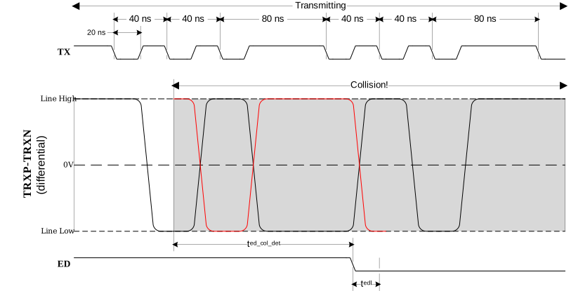
| Parameter | Symbol | Min | Typ | Max | Units | Additional Information |
|---|---|---|---|---|---|---|
| Collision detection time |
ted_col_det | — | — | 4500 | ns | Measured from start of the corrupted transmission signal at the MDI to the low assertion of ED |
| Minimum Time ED remains low after collision detected |
tedl | 21 | — | — | ns |
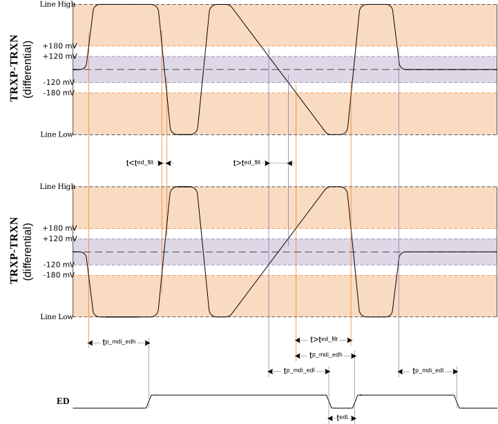
| Parameter | Symbol | Min | Typ | Max | Units | Additional Information |
|---|---|---|---|---|---|---|
| Delay from MDI to ED high |
tp_mdi_edh | — | — | 130 | ns |
Measured from a TRXP/N rising voltage crossing +180 mV or a TRXP/N falling voltage crossing -180 mV to rising edge crossing 50% level on ED |
| Delay from MDI to ED low |
tp_mdi_edl | — | — | 130 | ns |
Measured from a TRXP/N rising voltage crossing +120 mV or a TRXP/N falling voltage crossing -120 mV to falling edge crossing 50% level on ED |
| ED response filter time |
ted_filt | 21 | — | 39 | ns |
Filter time when the TRXP/N voltage is outside the +180 mV / -180 mV window or is inside the +120 mV / -120 mV window If the filter time is not reached, the ED pin remains HIGH. |
| ED low pulse time |
tedl | 28 | — | — | ns |
Minimum low time ED after no carrier detection |
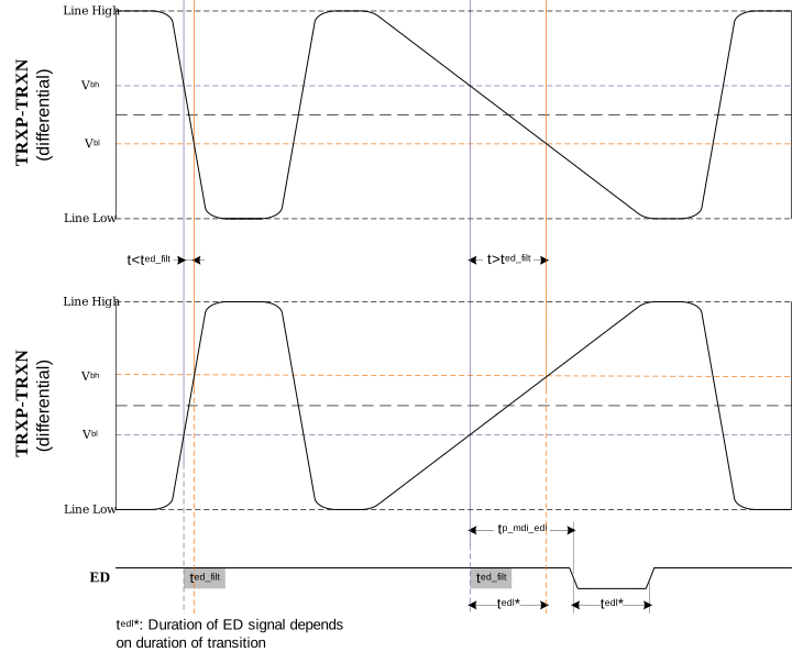
| Parameter | Symbol | Min | Typ | Max | Units |
|---|---|---|---|---|---|
| ED window amplitude | (Vbh - Vbl) | 270 | 320 | 330 | mV |
| ED window offset | (Vbh + Vbl) | -30 | 7 | 30 | mV |
Signal Timing during the Transition to TRANSMITTING State
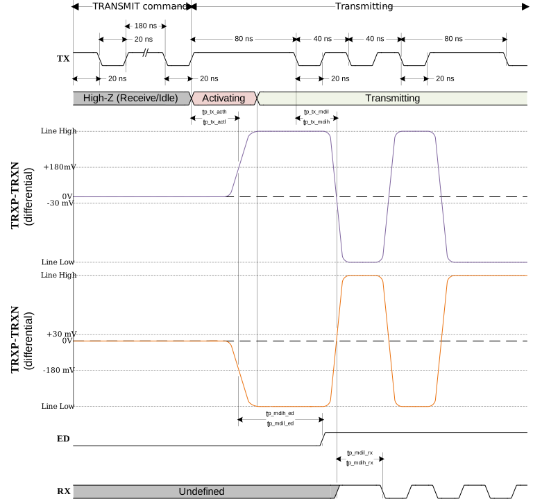
| Parameter | Symbol | Min | Typ | Max | Units | Additional Information | |
|---|---|---|---|---|---|---|---|
| Transmitter specification from NORMAL to TRANSMITTING state | |||||||
| Propagation delay from rising edge on TX to rising edge on TRXP/N when starting transmission |
tp_tx_acth | — | — | 50 | ns |
Measured from rising edge crossing 50% level on TX at the end of TRANSMIT command to a TRXP/N rising voltage crossing of +180 mV starting from High-Z | |
| Propagation delay from rising edge on TX to falling edge on TRXP/N when starting transmission |
tp_tx_actl | — | — | 50 | ns |
Measured from rising edge crossing 50% level on TX at the end of TRANSMIT command to a TRXP/N falling voltage crossing of -180 mV starting from High-Z | |
| ED specification from NORMAL to TRANSMITTING state | |||||||
| Propagation delay from TRXP/N rising edge to ED high |
tp_mdih_ed | — | — | 130 | ns |
Measured from a TRXP/N rising voltage crossing +180 mV to rising edge crossing 50% level on ED | |
| Propagation delay from TRXP/N falling edge to ED high |
tp_mdil_ed | — | — | 130 | ns |
Measured from a TRXP/N falling voltage crossing -180 mV to rising edge crossing 50% level on ED | |
|
Notes:
| |||||||
Signal Timing during the Transition to NORMAL State
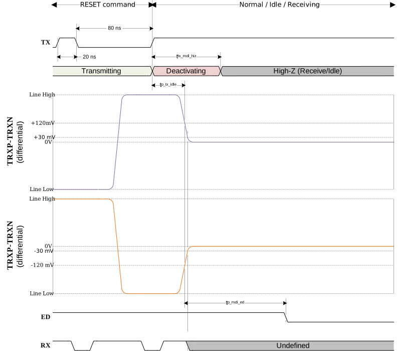
| Parameter | Symbol | Min | Typ | Max | Units | Additional Information | |
|---|---|---|---|---|---|---|---|
| Transmitter specification from TRANSMITTING to NORMAL state | |||||||
| Delay from end of reset command to 0 signal on TRXP/N |
tp_tx_idle | — | — | 65 | ns |
Measured from rising edge crossing 50% level on TX at the end of RESET command to a TRXP/N falling voltage crossing of +120 mV or a TRXP/N rising voltage crossing of -120 mV | |
| Delay from end of reset command to high impedance on TRXP/N |
ttx_mdi_hiz | — | — | 110 | ns |
Measured from rising edge crossing 50% level on TX at the end of RESET command to driving TRXP/N with high impedance (> minimum specified input impedance) | |
| ED specification from TRANSMITTING to NORMAL state | |||||||
| Propagation delay from 0 signal on TRXP/N to ED low |
tp_mdi_ed | — | — | 130 | ns |
Measured from a TRXP/N falling voltage crossing of +120 mV or a TRXP/N rising voltage crossing of -120 mV to falling edge crossing 50% level on ED | |