
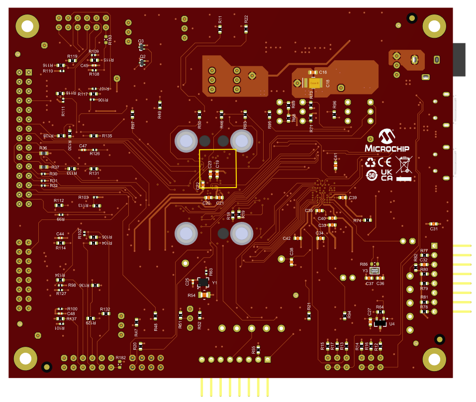
4.4.2 Revision R2 - Filtering Capacitors
For some development use cases, it is necessary to interface with an external board such as the UMFT4222EV-D - FT4222H evaluation module, USB Hi-Speed to SPI/I2C Master/Slave. It has been found that the performance of the interface can be improved by adding a small filtering capacitor to the SPI0PER_nCS chip select line. The schematic location of the capacitors is identical between the R2 and R3 revisions of the board and can be seen in figure Figure 4-10
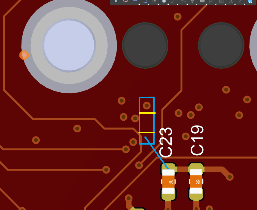
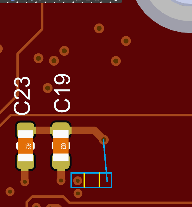
A value of 100 nF was used in each location. Cap C51 was added between the GPIO250/SPI0PER_nCS line and GND. Cap C52 was added between the GPIO024/SPI1PER_nCS line and GND. With these additions, SPT works reliably up to 30 MHz, and the drive strength was tested with max 16 mA.
The best location for C51 and C52 is on the back side of the board, underneath the CEC, as shown below. This image is a 3D rendering of the R2 revision development board.
The following images show a detailed view of the required modifications in the figure below. These are based on the database for the R2 version of the evaluation board. The blue box and wire represent the location of the capacitor and the addition of solder and/or wire needed to complete the modifications.
 |
 |