7 Hardware Peripherals
Kit hardware peripherals overview.
7.1 LED
One yellow user LED is available on the PIC32CM PL10 Curiosity Nano board. It can be controlled by either GPIO or PWM. Driving the connected I/O line to GND will activate the LED.
| MCU Pin | Description | Default Connection |
|---|---|---|
| PB02 | User LED (yellow), active low |
|
7.2 Mechanical Switch
The PIC32CM PL10 Curiosity Nano board has one mechanical switch - a generic, user-configurable switch. Pressing it connects the I/O pin to ground (GND).
| MCU Pin | Description | Default Connection |
|---|---|---|
| PB03 | User switch (SW0), supports DGI event monitoring |
|
7.3 Crystal
The PIC32CM PL10 Curiosity Nano Board has a 32.768 kHz crystal mounted. The crystal is not connected to the target MCU by default, as the GPIO pins are routed to the edge connector.
| MCU Pin | Description | Default Connection |
|---|---|---|
| PA24 | Crystal output, XTAL32K1 | Edge connector |
| PA25 | Crystal input, XTAL32K2 |
- Disconnect the two I/O lines routed to the edge connector by cutting the two cut straps on the bottom side of the board, J107 and J108.
- Connect the two I/O lines to the crystal by soldering a blob on each circular solder point on the top of the board (J109 and J110).
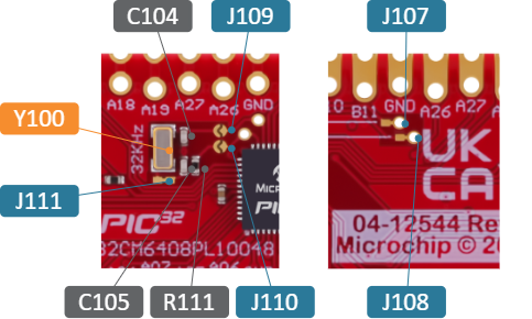
The 32.768 kHz crystal has a cut strap (J111), which can be used to measure the oscillator safety factor. This is done by cutting the strap and adding a 0402 SMD resistor across it. The AN2648 application note from Microchip contains more information about oscillator allowance and safety factors.
7.4 Touch Button
The PIC32CM PL10 Curiosity Nano board has a single capacitive touch button with an active shield. For details on configuration and usage, refer to the Peripheral Touch Controller (PTC) chapter in the PIC32CM PL10 device data sheet.
| MCU Pin | Description | Default Connection |
|---|---|---|
| PB08 | Shield connection for improved noise immunity |
|
| PB09 | Capacitive touch connection |
|
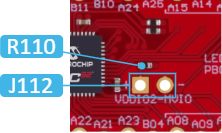
7.5 Multi-Voltage I/O
The target MCU includes a Multi-Voltage I/O (MVIO) domain powered through the VDDIO2 pin. Pins PA08–PA15 are exclusively powered by VDDIO2. If VDDIO2 is not supplied, these I/O pins will not operate.
On the PIC32CM PL10 Curiosity Nano board, VCC_TARGET supplies VDDIO2 by default. Removing the 0Ω resistor R110 disconnects the default power connection. After the removal, an external power supply can power the MVIO pins through the 1x2-100mil footprint (J112).
- Always disconnect the board from all power sources before making changes
- To prevent damage to the board, remove R110 before applying external voltage to VDDIO2
- The MVIO circuit lacks reverse polarity protection. Incorrect connections at J112 may permanently damage the board.