
6.3 Temperature and Voltage Sensor
(Ask a Question)Each device is equipped with a Temperature and Voltage Sensor (TVS). It reports die temperature and voltages of—VDD (1.0V), VDD18 (1.8V), and VDD25 (2.5V)—device supply rails in digital form to the FPGA fabric. TVS is implemented using a 4-channel ADC and the channel information is given as follows:
- Channel 0 - VDD (1V) voltage supply
- Channel 1 - VDD18 (1.8V) voltage supply
- Channel 2 - VDD25 (2.5V) voltage supply
- Channel 3 - die temperature
The TVS outputs a 16-bit encoded value that represents voltage or temperature, and corresponding channel number. The temperature and voltage information is translated into standard temperature and voltage values. The temperature channel output is also given to a comparator residing within the system controller that raises an alarm if the temperature is not between the maximum and minimum threshold levels specified by the user.
The voltage channel's 16-bit output value is represented in millivolts (mV) and can be decoded as listed in the following table. For example, the voltage channel's output value of 0x385E implies 1803.75 mV.
| Bit Number | Description |
|---|---|
| 15 | Signed bit |
| [14:3] | Integer value of voltage |
| [2:0] | Fractional value of voltage |
The temperature channel's 16-bit output value is represented in Kelvin and can be decoded as listed in the following table. For example, the temperature channel's output value of 0x133B implies 307.6875 Kelvin.
| Bit Number | Description |
|---|---|
| 15 | Reserved |
| [14:4] | Integer value of temperature |
| [3:0] | Fractional value of temperature |
The TVS is accessible by instantiating PF_TVS macro in the design, see the following figure.
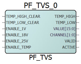
The following table lists the PF_TVS macro ports and their description.
| Port Name | Direction | Description |
|---|---|---|
| ENABLE_1V | Input | VDD (1V) channel enable signal |
| ENABLE_18V | Input | VDD18 (1.8V) channel enable signal |
| ENABLE_25V | Input | VDD25 (2.5V) channel enable signal |
| ENABLE_TEMP | Input | Temperature channel enable signal |
| TEMP_HIGH_CLEAR | Input | Control input to clear TEMP_HIGH flag |
| TEMP_LOW_CLEAR | Input | Control input to clear TEMP_LOW flag |
| VALID | Output | Asserted after channel/value changes |
| CHANNEL[1:0] | Output | Indicates available channel data on VALUE[15:0], held until the next conversion completes |
| VALUE[15:0] | Output | Channel data, held until the next conversion completes |
| TEMP_HIGH | Output | Set when temperature is above the high level threshold |
| TEMP_LOW | Output | Set when temperature is below the low level threshold |
| ACTIVE | Output | Indicates that the TVS is active |
The data present on the VALUE and CHANNEL outputs is valid only when the VALID output is asserted. When a channel is disabled by deasserting the corresponding channel enable input, then the channel data present on the outputs is not valid even if the VALID output is asserted.
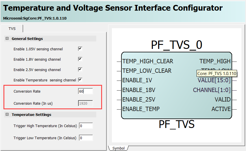
The following figure shows the TVS configurator. In General Settings, users has the option to choose channels for conversion and conversion rate options. In Temperature Settings, user can specify the threshold values for Trigger High Temperature and Trigger Low Temperature alarm flags generation. The temperature ranges from -55 °C to 125 °C. This is enabled only when the temperature channel sensing is enabled. The temperature high and low alarm flags (TEMP_HIGH and TEMP_LOW) can only be cleared by the user once the measured temperature returns to normal.
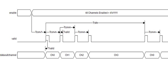
The following figure shows the TVS conversion sequence when all the channels are enabled. The time between subsequent channel conversions is called conversion delay (Tconvn). The time between the start of the first set of conversions to the start of the next set is called conversion rate (Trate).
- Conversion rate = conversion rate parameter × 32 µs.
- Conversion rate parameter ≥ Number of channels enabled × 15
For example, if one channel is enabled then the minimum conversion rate parameter is equal to 15, which means the conversion rate is 480 µs. If all four channels are enabled then the minimum conversion rate parameter is equal to 60, which mean the conversion rate is 1920 µs.
See respective PolarFire FPGA Datasheet or PolarFire SoC Datasheet for accuracy and electrical characteristics of TVS.