1 Electrical Characteristics
Absolute Maximum Ratings
- VDD
- 6.0V
- Voltage at All Input/Output Pins
- GND – 0.3V to 6.0V
- Storage Temperature
- -65°C to +150°C
- Ambient Temperature with Power Applied
- -40°C to +125°C
- Junction Temperature (TJ)
- +150°C
- ESD Protection on All Pins (HBM:MM)
- (4 kV:400V)
- Latch-up Current at Each Pin (+25°C)
- ±200 mA
: Stresses above those listed under “Maximum ratings” may cause permanent damage to the device. This
is a stress rating only and functional operation of the device at those or any other conditions above those indicated in the operational
listings of this specification is not implied. Exposure to maximum rating conditions for extended periods may affect device
reliability.
| Electrical Specifications: Unless otherwise indicated, VDD = 2.7V to 5.5V, GND = Ground and TA = -40°C to +125 °C. | ||||||
|---|---|---|---|---|---|---|
| Parameters | Sym. | Min. | Typ. | Max. | Unit | Conditions |
| Temperature Sensor Accuracy | ||||||
| -20°C < TA ≤ +100 °C | TACY | -0.5 | ±0.25 | +0.5 | °C | VDD = 3.3V (Note 1) |
| -40°C < TA ≤ +125 °C | -1.0 | ±0.25 | +1.0 | °C | ||
| Accuracy Drift | TDRIFT | — | +0.05 | — | °C | VDD = 3.3V (Note 2) |
| Accuracy Repeatability | TREPEAT | — | ±0.0625 | — | °C | 48 hours at +55°C, VDD = 3.3V |
| Temperature Conversion Time | ||||||
| 0.5°C/bit | tCONV | — | 30 | — | ms | 33s/sec (typical) |
| 0.25°C/bit | — | 65 | — | ms | 15s/sec (typical) | |
| 0.125°C/bit | — | 130 | — | ms | 7s/sec (typical) | |
| 0.0625°C/bit | — | 250 | — | ms | 4s/sec (typical) | |
| Power Supply | ||||||
| Operating Voltage Range | VDD | 2.7 | — | 5.5 | V | |
| Operating Current | IDD | — | 200 | 400 | µA | |
| Shutdown Current | ISHDN | — | 0.1 | 2 | µA | |
| Power-on Reset (POR) | VPOR | — | 2.2 | — | V | Threshold for falling VDD |
| Power Supply Rejection | Δ°C/ΔVDD | — | -0.1 | — | °C/V | VDD = 2.7V to 5.5V, TA = +25°C |
| Alert Output (open-drain output, external pull-up resistor required), see Alert Output Configuration | ||||||
| High-Level Current (leakage) | IOH | — | — | 1 | µA | VOH = VDD (Active-Low, Pull-up Resistor) |
| Low-Level Voltage | VOL | — | — | 0.4 | V | IOL= 3 mA (Active-Low, Pull-up Resistor) |
| Thermal Response, from +25°C (air) to +125°C (oil bath) | ||||||
| 8L-DFN | tRES | — | 0.7 | — | s | Time to 63% (+89°C) |
| 8L-MSOP | — | 1.4 | — | s | ||
Note:
- Accuracy specification includes life time drift.
- Using Accelerated Life Cycle, equivalent of 12 years of operation at +55°C.
| Electrical Specifications: Unless otherwise indicated, VDD = 2.7V to 5.5V, GND = Ground and TA = -40°C to +125 °C. | ||||||
|---|---|---|---|---|---|---|
| Parameters | Sym | Min | Typ | Max | Units | Conditions |
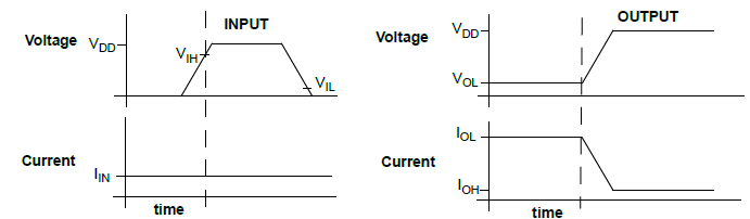
| Serial Input/Output (SCL, SDA, A0, A1, A2) | ||||||
| Input | ||||||
| High-Level Voltage | VIH | 0.7 VDD | — | VDD | V | |
| Low-Level Voltage | VIL | GND | — | 0.3 VDD | V | |
| Input Current | IIN | — | — | ±5 | µA | |
| Output (SDA) | ||||||
| Low-Level Voltage | VOL | — | — | 0.4 | V | IOL= 3 mA |
| High-Level Current (leakage) | IOH | — | — | 1 | µA | VOH = 5.5V |
| Low-Level Current | IOL | 6 | — | — | mA | VOL = 0.6V |
| SDA and SCL Inputs | ||||||
| Hysteresis | VHYST | — | 0.05 VDD | — | V | |
| Spike Suppression | tSP | — | — | 50 | ns | |
| Capacitance | CIN | — | 5 | — | pF | |
| Electrical Specifications: Unless otherwise indicated, VDD = 2.7V to 5.5V and GND = Ground. | ||||||
|---|---|---|---|---|---|---|
| Parameters | Sym | Min | Typ | Max | Units | Conditions |
| Temperature Ranges | ||||||
| Specified Temperature Range | TA | -40 | — | +125 | °C | (Note 1) |
| Operating Temperature Range | TA | -40 | — | +125 | °C | |
| Storage Temperature Range | TA | -65 | — | +150 | °C | |
| Thermal Package Resistances | ||||||
| Thermal Resistance, 8L-DFN | θJA | — | 68 | — | °C/W | |
| Thermal Resistance, 8L-MSOP | θJA | — | 211 | — | °C/W | |
Note: Operation in this range must not cause TJ to exceed Maximum Junction Temperature
(+150°C).
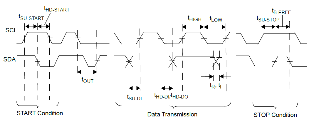
| Electrical Specifications: Unless otherwise indicated, VDD = 2.7V to 5.5V, TA = -40°C to +125°C, GND = Ground and CL = 80 pF. (Note 1) | |||||
|---|---|---|---|---|---|
| Parameters | Sym | Min | Max | Units | Conditions |
| 2-Wire SMBus/I2C Interface (Note 1) | |||||
| Serial Port Clock Frequency | fSC | 0 | 400 | kHz | (Note 2, 4) |
| Low Clock | tLOW | 1300 | — | ns | (Note 2) |
| High Clock | tHIGH | 600 | — | ns | (Note 2) |
| Rise Time | tR | 20 | 300 | ns | |
| Fall Time | tF | 20 | 300 | ns | |
| Data in Setup Time | tSU-DI | 100 | — | ns | (Note 3) |
| Data In Hold Time | tHD-DI | 0 | — | ns | (Note 5) |
| Data Out Hold Time | tHD-DO | 200 | 900 | ns | (Note 4) |
| Start Condition Setup Time | tSU-START | 600 | — | ns | |
| Start Condition Hold Time | tHD-START | 600 | — | ns | |
| Stop Condition Setup Time | tSU-STOP | 600 | — | ns | |
| Bus Free | tB-FREE | 1300 | — | ns | |
| Time-out | tOUT | 25 | 35 | ms | |
| Bus Capacitive Load | Cb | — | 400 | pf | |
Note:
- All values referred to VIL MAX and VIH MIN levels.
- If tLOW > tOUT or tHIGH > tOUT, the temperature sensor I2C interface will time-out. A Repeat Start command is required for communication.
- This device can be used in a Standard mode I2C bus system, but the requirement, tSU-DI ≥ 100 ns, must be met. This device does not stretch the SCL Low time.
- As a transmitter, the device provides internal minimum delay time, tHD-DO MIN, to bridge the undefined region (min. 200 ns) of the falling edge of SCL, tF MAX, to avoid unintended generation of Start or Stop conditions.
- As a receiver, SDA should not be sampled at the falling edge of SCL. SDA can transition tHD-DI after SCL toggles Low.