
3 Packaging Information
CMOS Package
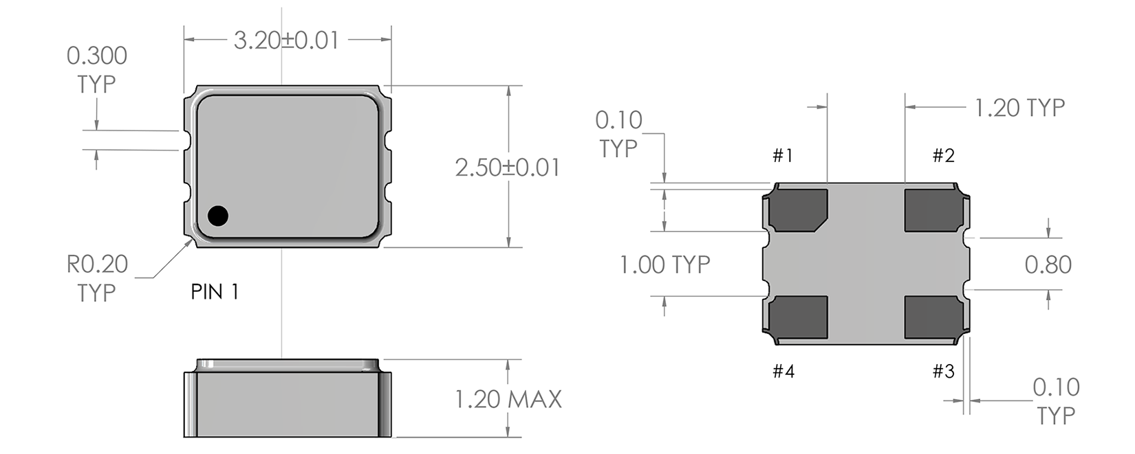
| Package Code | Length“L” | Width “W” | Height“H” |
|---|---|---|---|
| 0 | 3.2mm ±0.2mm | 2.5mm ±0.2mm | 1.2mm max. |
| Pin Number | Pin Description |
|---|---|
| 1 |
Enable/Disable or N/C Output active = Floating or Voltage Applied |
| 2 | Ground (Case) |
| 3 | RF Output |
| 4 | Supply |
Note: Package standard termination finish: Au 12-39 microinches
over Nickel 50 microinches minimum.
Important: Overall package thickness
tolerance will be increased from ±.007 to ±.015 inches when
pads are solder coated.
LVDS Package
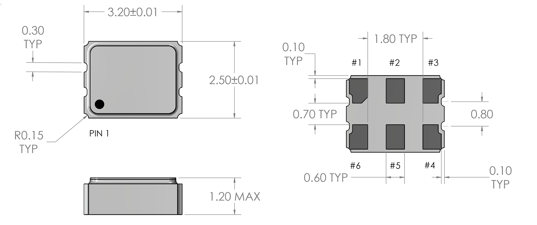
| Package Code | Length“L” | Width “W” | Height“H” |
|---|---|---|---|
| 1 | 3.2mm ±0.2mm | 2.5mm ±0.2mm | 1.2mm max. |
| Pin Number | Pin Description |
|---|---|
| 1 |
Enable/Disable or N/C Output active = Floating or Voltage Applied |
| 2 | N/C |
| 3 | Ground (Case) |
| 4 | LVDS+ |
| 5 | LVDS- |
| 6 | Supply |
Note: Package standard termination finish: Au 12-39 microinches
over Nickel 50 microinches minimum.
Important: Overall package thickness
tolerance will be increased from ±.007 to ±.015 inches when
pads are solder coated.