
1 Performance Specifications
| Parameter | Min. | Typ. | Max. | Units | Condition |
|---|---|---|---|---|---|
| Overall Tolerance (Includes Operation Temperature and Initial Accuracy) | −25 | — | 25 | ppm |
See Table I under Product Identification System Referenced to nominal frequency @ +25°C |
| −50 | 50 | ||||
| –65 | 65 | ||||
| −100 | 100 | ||||
| vs. supply Voltage Change | −2 | — | 2 | ppm | VS ±5% |
| vs. Load Change | −1 | — | 1 | ppm | Load ±5% |
| vs. Aging/Year (Year 1) | −3 | — | 3 | ppm | After 30 days of operation |
| Parameter | Min. | Typ. | Max. | Units | Condition |
|---|---|---|---|---|---|
|
Supply Voltage | 3.135 | 3.3 | 3.465 | VDC | — |
| 2.375 | 2.5 | 2.625 | VDC | — | |
| 1.710 | 1.8 | 1.890 | VDC | — |
| Parameter | Min. | Typ. | Max. | Units | Output | Frequency Range |
|---|---|---|---|---|---|---|
|
Current Consumption No Load VS = 3.465 VDC | — | — | 3 | mA | CMOS | 1.25MHz to < 12MHz |
| 5 | mA | 12MHz to < 48MHz | ||||
| 10 | mA | 48MHz to < 85MHz | ||||
| 15 | mA | 85MHz to 135MHz | ||||
| 40 | mA | LVDS | 100MHz to 250MHz | |||
|
Current Consumption No Load VS = 2.625 VDC | — | — | 2 | mA | CMOS | 1.25MHz to < 12MHz |
| 4 | mA | 12MHz to < 48MHz | ||||
| 9 | mA | 48MHz to < 85MHz | ||||
| 12 | mA | 85MHz to 135MHz | ||||
| 35 | mA | LVDS | 100MHz to 250MHz | |||
|
Current Consumption No Load VS = 1.89 VDC | — | — | 1.5 | mA | CMOS | 1.25MHz to < 12MHz |
| 3 | mA | 12MHz to < 48MHz | ||||
| 8 | mA | 48MHz to < 85MHz | ||||
| 10 | mA | 85MHz to 135MHz | ||||
| 25 | mA | LVDS | 10MHz to 175MHz |
| Parameter | Min. | Typ. | Max. | Units | Condition |
|---|---|---|---|---|---|
| Frequency Range | 1.3 | — | 135 | MHz | VDD = 1.8V, 2.5V, 3.3V |
| Load | — | — | 15 | pF | — |
| Signal Level (VOL) | — | — | 0.3 | VDC | VS= 3.3V and 15pF load |
| 0.25 | VDC | VS = 2.5V and 15pF load | |||
| 0.18 | VDC | VS = 1.8V and 15pF load | |||
| Signal Level (VOH) | 3 | — | — | VDC | VS = 3.3V and 15pF load |
| 2.3 | VDC | VS = 2.5V and 15pF load | |||
| 1.6 | VDC | VS = 1.8V and 15pF load | |||
|
Rise/Fall Times (10% to 90%) | — | — | 10 | ns | 1.0MHz to 23.9MHz |
| 6 | ns | 24.0MHz to 79.9MHz | |||
| 3 | ns | 80.0MHz to 135.0MHz | |||
| Duty Cycle | 45 | 50 | 55 | % | Measured at 50% of VDD |
| Parameter | Min | Typ | Max | Units | Condition |
|---|---|---|---|---|---|
| Frequency Range | 100 | — | 250 | MHz | VDD = 2.5V or 3.3V |
| Frequency Range | 100 | — | 175 | MHz | VDD = 1.8V |
| Signal Level (VOL) | — | 1.2 | — | VDC | RL = 100Ω |
| Signal Level (VOH) | — | 1.4 | — | VDC | RL = 100Ω |
| Differential Voltage (VOD) | 250 | — | 460 | mV | RL = 100Ω |
| Offset Voltage (VOS) | 1.13 | — | 1.45 | V | RL = 100Ω |
| Rise/Fall Times | — | 600 | 1000 | ps | 20% to 80% of VOD |
| Duty Cycle | 45 | — | 55 | % | Measured at 50% of VOD |
Note: Please email VOP-Support@microchip.com for technical questions, sales, or other product
support.
 |  |
 |  |
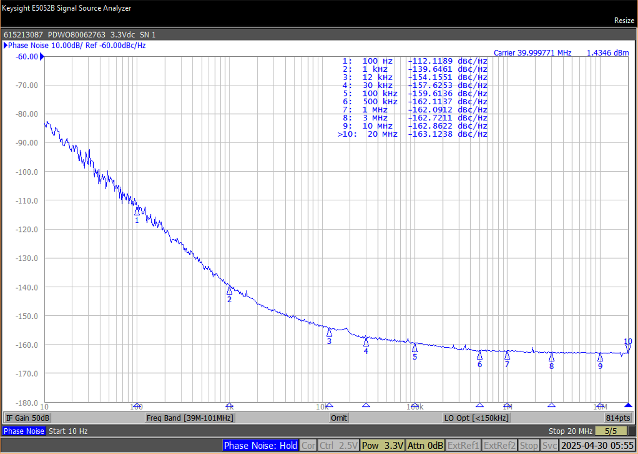 | 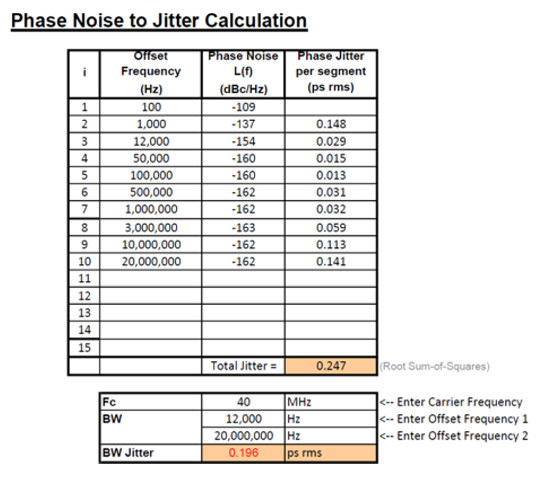 |
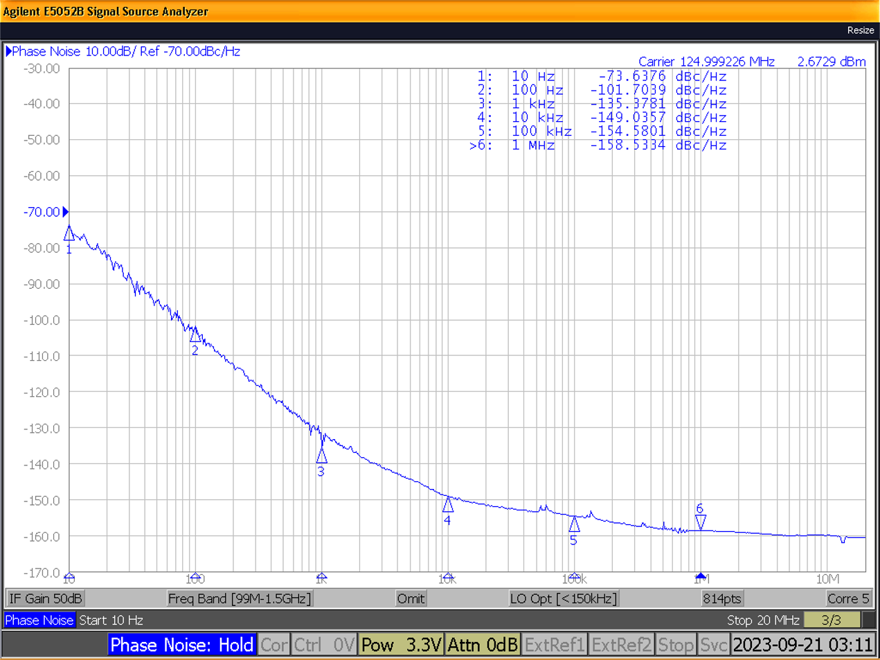 | 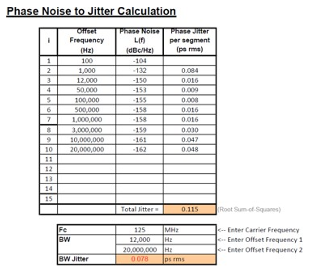 |
| Parameter | Conditions | Additional Notes |
|---|---|---|
| Screening | Microchip Verification (Standard “X”) | See the following table for Tests |
| Class B, MIL-PRF-55310 (Optional) | See the following table for Tests | |
| Output Enable | Logic “0” input == Output disabled (Tri-state) | — |
| Logic “1” or floating input == Output enabled | ||
| Weight | < 2 grams | — |
| Processing and Packing | Tape and Reel | — |
| RoHS Compliance | RoHS 6 | Unless Sn/Pb solder coated |
| REACH Compliance | Yes | — |
| Solder Coated Pads | Sn63/Pb37 Solder (Optional) | See Package Code in Part Number |
| Moisture Sensitivity Level (MSL) | 1 | Ceramic package, Seam sealed |
| MTBF/FIT (Generic) | 480,000,000 Hours |
MIL-HBK-217, Hybrid, Space Flight, Commercial Contact Factory for Custom MTBF/FIT |
| ECCN | EAR99 | — |
| Software 3D Model | IGS/STEP file | Contact VOP-Support@microchip.com |
| Test | Test Conditions |
|---|---|
| Internal Visual Inspection | MIL-STD-883, Methods 2017, 2032 |
| Stabilization Bake | MIL-STD-883, Method 1008, Condition C, 150°C, 24 hours minimum |
| Temperature Cycling | MIL-STD-883, Method 1010, Condition B |
| High-Temperature Reflow | 2 cycles of solder reflow profile, SnPb Standard, See Section 4 for profile |
| Seal Test (Fine Leak) | MIL-STD-883, Method 1014, Condition A2, Class B |
| Seal Test (Gross Leak) | MIL-STD-883, Method 1014, Condition C |
| Test | Test Conditions |
|---|---|
| Internal Visual Inspection | MIL-STD-883, Methods 2017, 2032 |
| Stabilization Bake | MIL-STD-883, Method 1008, Condition C, 150ºC, 24 hours min |
| Temperature Cycling | MIL-STD-883, Method 1010, Condition B |
| High-Temperature Reflow | 2 cycles of solder reflow profile, SnPb Standard, See last page for profile |
| Constant Acceleration | MIL-STD-883, Method 2001, Condition A, Y1 Plane only |
| Seal Test (Fine Leak) | MIL-STD-883, Method 1014, Condition A2, Class B |
| Seal Test (Gross Leak) | MIL-STD-883, Method 1014, Condition C |
| Burn-In | 160 hours minimum at 125°C, nominal voltage, specified load |
| External Visual Inspection | MIL-STD-883, Method 2009 |
| Parameter | Min. | Typ. | Max. | Units | Condition |
|---|---|---|---|---|---|
| Supply Voltage | −0.3 | — | 4 | VDC | — |
| Mechanical Shock | 1000 | G | MIL-STD-202, 0.5ms half-sine pulse | ||
| ESD | 2000 | Volts | HBM per MIL-STD-883, Method 3015 | ||
| Operable Temperature Range | −55 | — | 125 | °C | Operable temperature range implies the device will continue to operate with no long-term damage to unit; however, it may not be specification-compliant outside the operating temperature range. |