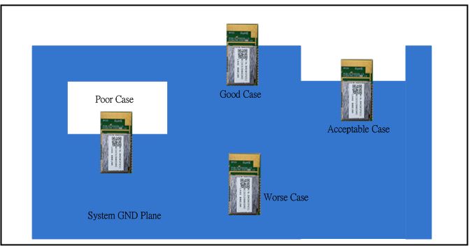
On the main PCB, the areas under the antenna should not contain any top,
inner layer, or bottom copper as shown in the below figure. A low‐impedance ground plane
will ensure the best radio performance (best range, lowest noise). The ground plane can
be extended beyond the minimum recommended as needed for the main PCB EMC noise
reduction. For the best range performance, keep all external metal at least 15 mm away
from the ceramic chip antenna. Figure 4-3. Module Placement
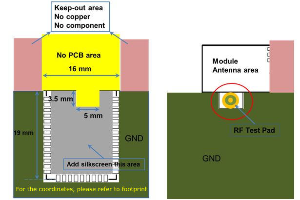
ExamplesFigure 4-4. GND Plane on Main Application
Board
The online versions of the documents are provided as a courtesy. Verify all content and data in the device’s PDF documentation found on the device product page.