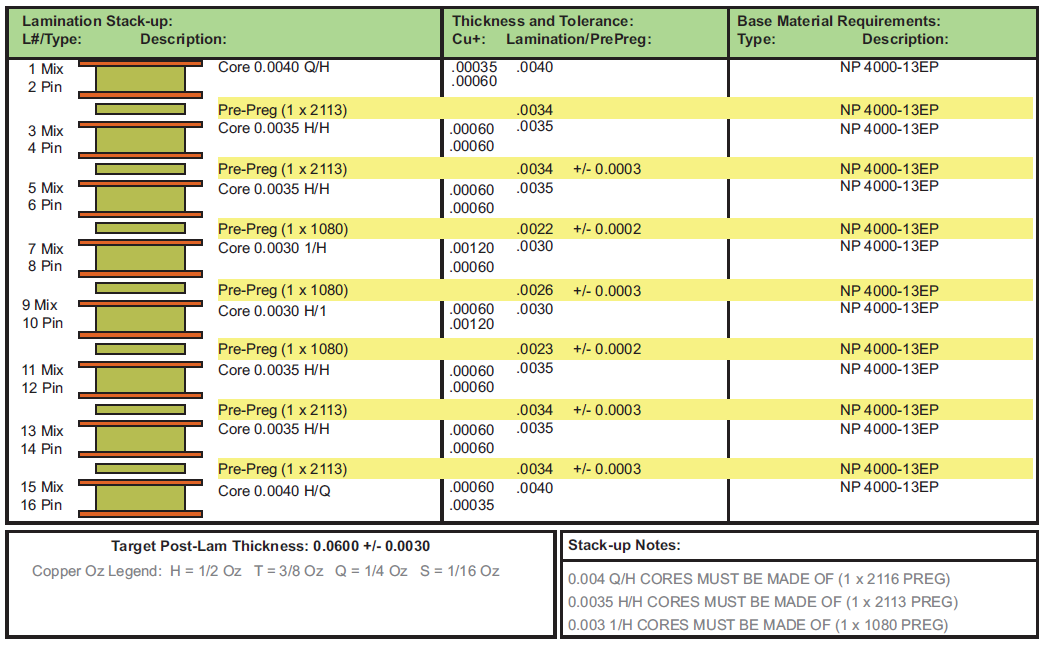
7 Appendix B: Stack-Up
(Ask a Question)A good stack-up leads towards better performance. The number of layers in the stack-up is dependent factors such as form factor of the board, number of signals to be routed, and power requirements. Therefore, the designer chooses how many layers the board requires. The SmartFusion2 Development Kit/IGLOO2 Evaluation Kit has 16-layer stack-up, as shown in Figure 7-1.
Utilizing upper power layers must be used for high priority supplies. High-switching current supplies must be placed vertically closer to the devices to decrease the distance the currents need to travel through vias. Ground planes are placed adjacent to the high transient current power planes to reduce inductance and couple the high-frequency noise.
It is good to have power and ground layers on side-by-side layer. The benefits of this inter-plane capacitance provide better decoupling at high frequencies. The effect of via on power pins is reduced by having a power plane near the device.
Signal integrity depends on how well the traces have controlled impedance, hence it is always recommended to have controlled impedance.
All critical high-speed signals like DDR and PCIe signals need to have ground reference. All signal layers must be separated from each other by ground or power planes. This minimizes crosstalk and provides balanced and clean transmission lines with properly controlled characteristic impedance between devices and other board components.
Best performance is obtained when using dedicated ground plane layers that are continuous across the entire board area. Power planes can provide adequate reference, however, the power planes must be related to the signals they serve to reference.
Slots must not interrupt the planes, or else they can possibly force current to find an alternate return path. This undesired return path could cause a localized bounce on the power or ground plane that can possibly be capacitive coupled to all signals adjacent to the planes.

