
3.1 Use Case 1: Stereo Class D Amplifier with External Differential Power Stage
The full_bridge_DMC2400UV_XXns_5%.sxsch and full_bridge_DMC2400UV_XXns_95%.sxsch files, available from the MPLAB® Mindi™ Analog Simulator Software Library (see the Appendix), implement in schematics the critical Class D modulation cases to feed the Mindi analog simulator.
These test benches simulate typical device behavior at ambient temperature. SPICE models for third-party components (here DMC2400UV_NMOS and DMC2400UV_PMOS) are available and can be installed by dragging and dropping them into the Mindi command shell, as documented in the SPICE Model Installation Guide. See the Appendix.
For a real-life circuit, it is recommended to start with the most conservative setting: a 20 ns non-overlap gap.
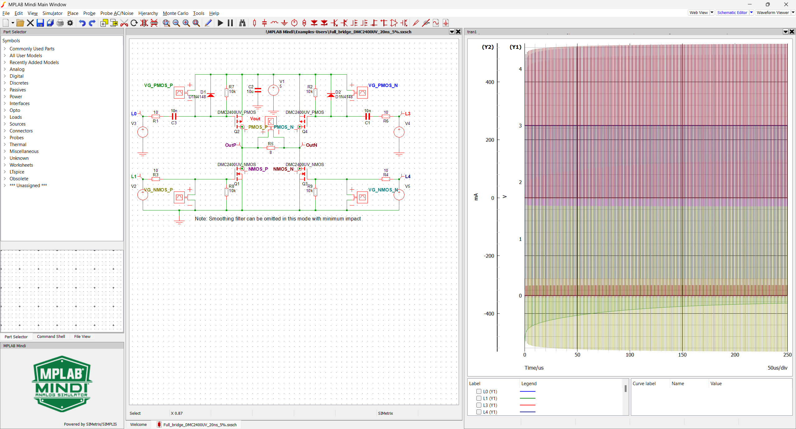
After the run completes, you can see the start-up transient. Zoom in on a single period in the Steady state, then stack the curves for clarity.
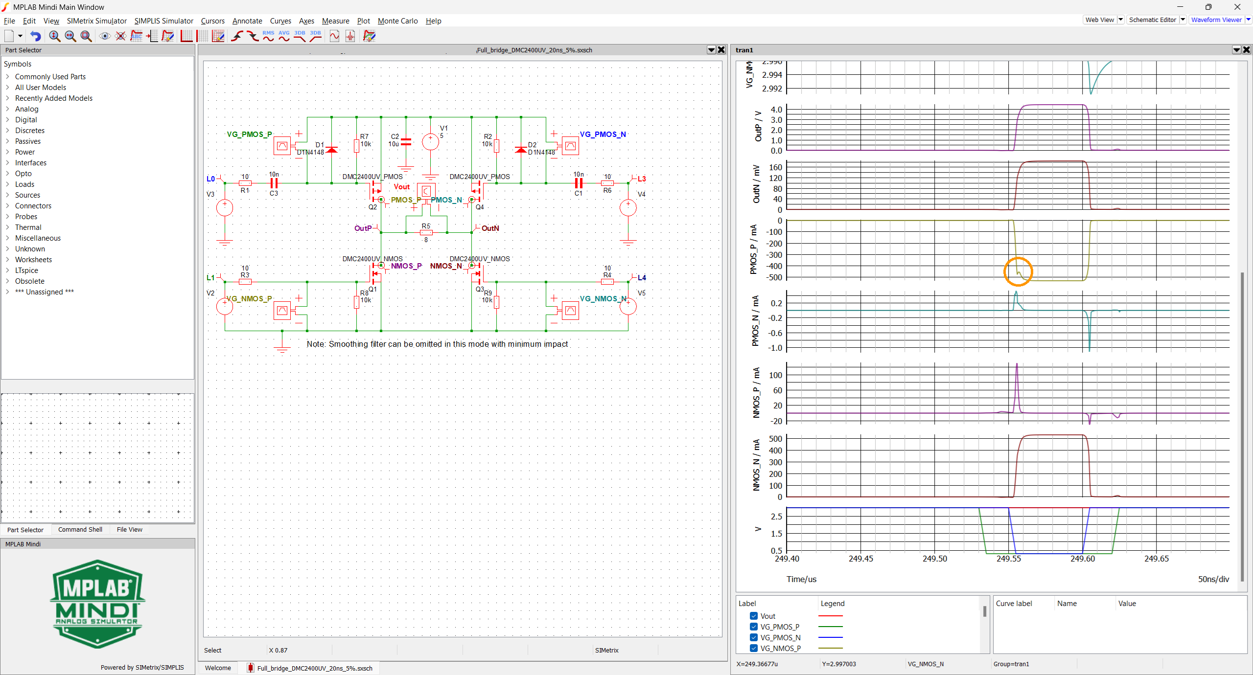
Globally, the waveforms show correct circuit behavior. The sharp output pulse is well rendered, and there is no violation of the device-rated current. The losses are aligned with the device data sheet values, but on the high side for the application. Simulation shows an ON resistance of ~1Ω in the PMOS (0.56V drop for 532 mA) and 0.35Ω in the NMOS (184 mV drop for 532 mA), which is aligned with the typical values specified in the data sheets. However, compared to an ideal 5V source, this generates a 27% loss in the maximum power delivered to the 8Ω load. The dissipated power is ~400 mW (shared between the two transistor pairs), not taking into account switching and inductor losses. With the 280°C/W Rth, the devices reach a ≥80°C temperature at ambient when run at maximum power.
Consequently, these power devices must be used with a maximum supply of 5.5V for an 8Ω load and 3.3V for a 4Ω load. They are not suitable for high-temperature operation.
The resulting waveforms show a very small spike in the positive driver's PMOS current during the transition from the Off to the On state. It coincides with the 130 mA peak in the NMOS current on the same side. This can be the cause of a shoot-through current.
In the test illustrated in the following figure, a 15 ns gap is set. The file Full_bridge_DMC2400UV_15ns_5%.sxsch is used.
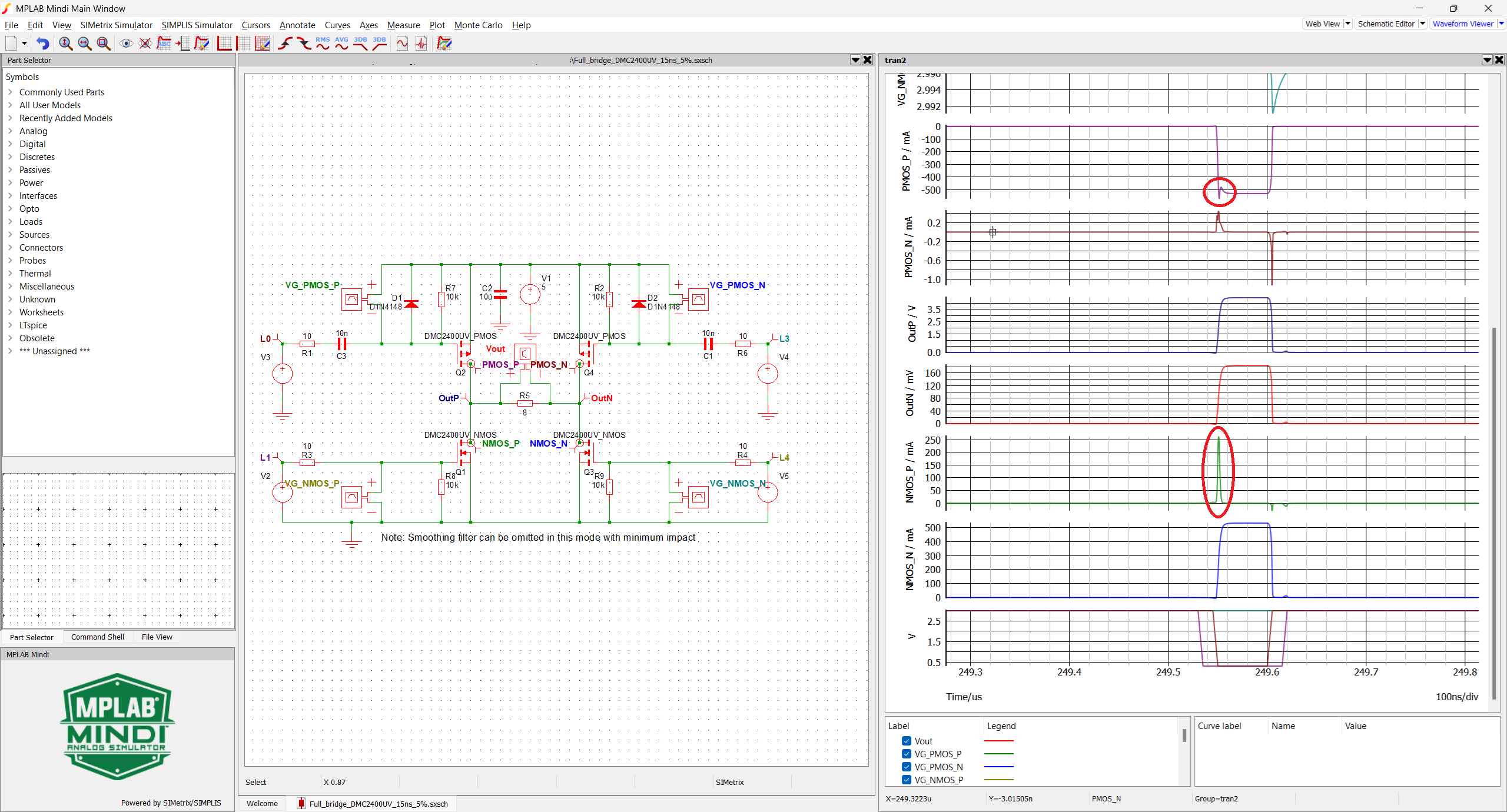
The current spike still does not exceed the maximum rating, but it is almost twice as high as in the 20 ns case, confirming that the result of the 20 ns case was likely to cause a shoot-through current. Since there is no benefit to the output waveform shape (it is not distorted with 20 ns, which would indicate that the gaps used are too wide), it is preferable to use the 20 ns setting.
The following figure illustrates a test with a 95% PWM duty cycle.
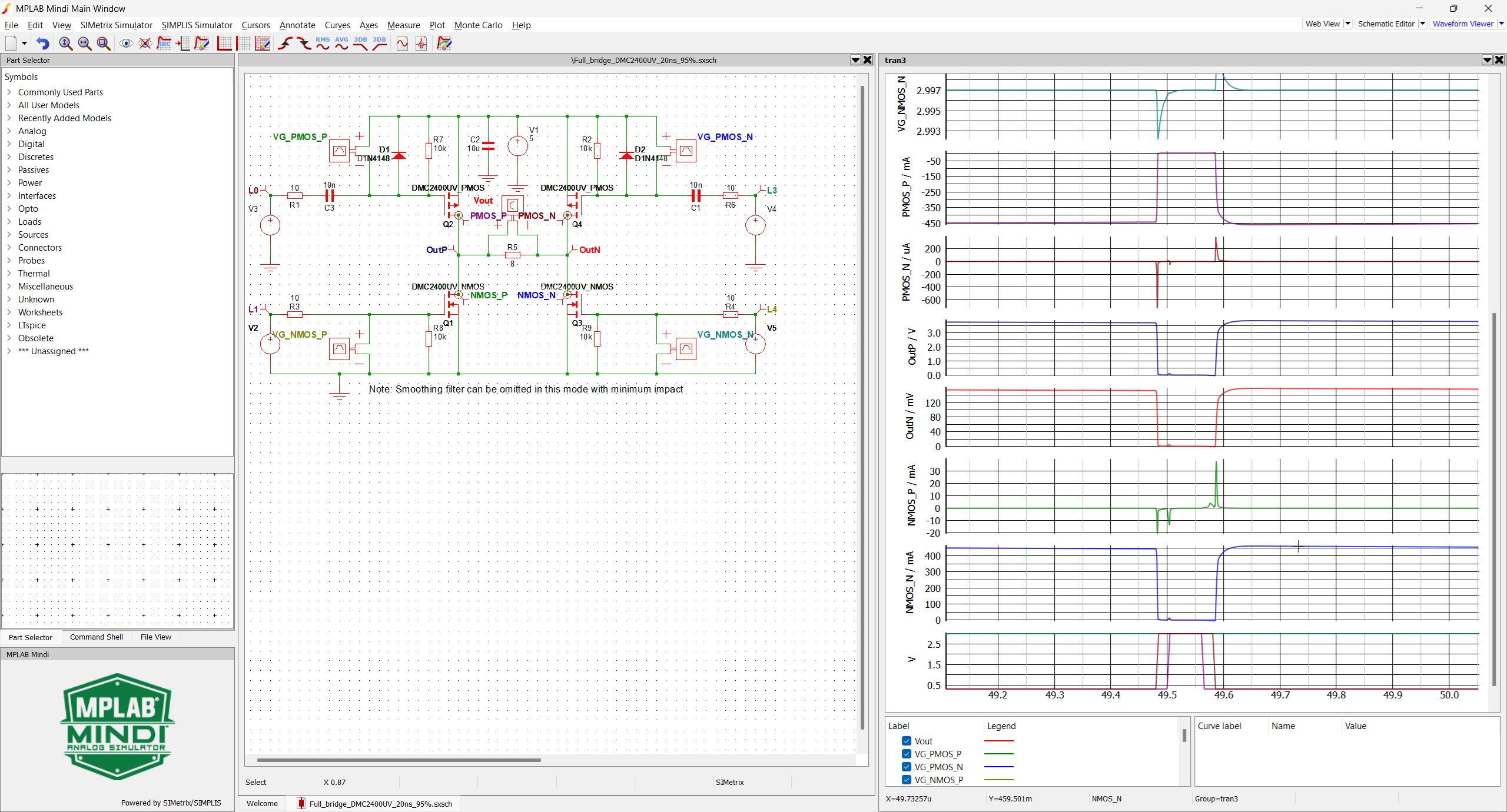
No particular issue is detected when using the 20 ns setting.