9 Advanced Topics
Additional reading for advanced users.
9.1 Clocking the Configurable Logic Block
How the CLB relates to clocks
The CLB peripheral receives its clock input from the source specified in the CLK field in the CLBCLK register which is written from the CPU. Consult the datasheet for available clock sources.
The CLB also includes a clock divider which must be configured along with the logic design, and is incorporated into the bitstream. The clock source can be divided by 1, 2, 4, 8, 16, 32, 64 or 128.
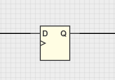
The CLB clock is distributed to all BLE flip-flops, so the entire logic design runs off the same clock. So although logic design schematics can include various flip-flop types, it is not possible to connect or configure an indivial clock source.

9.2 Preferences
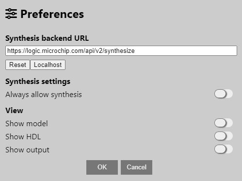
The preferences panel is accessed via the main drawer-menu.

| Option | Description |
|---|---|
| Synthesis backend URL | URL for the synthesis server. This should not be changed unless instructed to by Microchip support engineers. |
| Show model | The right-hand pane will show the "GUI model" of the current design - this is for internal debugging of the GUI. |
| Show HDL | The right-hand pane will show the intermediate HDL of the current design. This content will be sent to the backend for synthesis - it is for internal debugging of the interface between GUI and backend. |
| Show output | The right-hand pane will show output from the synthesis engine - this is for internal debugging of the backend logic-synthesis engine. |
9.3 Making Use of the Output ZIP
How to use the output
The synthesis process should always return a ZIP file with outputs.
The ZIP file is intended for the CLB Synthesizer Web version's users who want to convert a logic design into a bitstream.
- The resultant bitstream
- A basic CLB driver for configuring the peripheral
- Build artefacts
For further details, read the readme inside the ZIP.
9.4 Description of Output Files
After synthesis, a ZIP file containing many build artifacts can be downloaded. The filename prefix (XXX) is determined by the server in some cases.
- Root folder: outputs for use in bare-metal projects
- Build folder: debug artifacts from the build process
- Build/input folder: inputs passed into the server for processing
| Filename | Description |
|---|---|
| readme.txt | Instructions for bare-metal users |
| clb1.c; clb1.h | Driver for configuring and enabling the CLB |
| clb1_output_mappings.h | Header file defining output mappings from eh CLB to peripherals |
| bitstream.s | Bitstream in assembler format for embedding into a bare-metal project |
| input/*.v | Verilog representation of input design |
| input/*.xdc | Mappings to physical pins |
| input/project.json | Top level description of the design |
| input/stats.json | Statistical summary of the design |
| input/*.clb | Save-file for the design |
| XXX.inputs.json | List of design inputs in json format |
| XXX.outputs.json | List of design outputs in json format |
| XXX.bitstream.outputmappings.json | Peripheral output mappings in json format |
| XXX.bitstream | Raw bitstream words |
| XXX.bitstream.json | Bitstream words in json format |
| XXX.result.json | Entire operation output summary as json |
| XXX.json | json formatted netlist output from Yosys |
| XXX.v | Verilog netlist output from Yosys (before place and route) |
| XXX.netlist | Binary form of netlist |
| XXX.phys | Binary form of physical netlist |
| XXX.net | Packed netlist in XML format |
| XXX.net.post_routing | Post-routing packed netlist in XML format |
| XXX.place | Placer output report |
| XXX.route | Router output report |
| packaging_pin_util.rpt | Packing pin usage report |
| XXX.fasm | Output from FASM stage |
| XXX.svg | Diagramatic representation output from Yosys (generic) |
| XXX-2.svg | Alternative diagramatic representation output from Yosys (generic) |
| XXX.dot | Input to svg above |
| vpr_stdout.log | Place and route output |
| XXX.yosys.log | Log from Yosys synthesis stage |
| XXX.stderr.txt | Stderr output |
9.5 Synthesis and Place-and-Route Process
What goes on behind the scenes
Once an application has been captured in the CLB Synthesizer GUI, it needs to be converted into a configuration bitstream which can be loaded into the CLB module itself. This process is known as "synthesis", although it also includes place and route steps, and is done by Microchip's online web-service.
It is not necessary for a user to understand how this process works - a brief summary is given here for advanced or curious users.
How it works
- The schematic drawings of the CLB application are converted to equivalent Verilog descriptions which are then passed to the backend for processing.
- The first stage in the backend process is logic synthesis. Logic synthesis is a process of converting the Verilog textual representation of a logic design into a netlist which describes the hardware in equivalent logic gates and wires. Logic synthesis is done using Yosys Open SYnthesis Suite which is equipped with a plug-in that describes the actual structure of the logic elements in the CLB module. The output of the synthesis stage is a Verilog netlist.
- The next stage is place-and-route (PNR). During this stage the netlist elements are mapped into physical locations in the CLB array (placement), and interconnects are made between them (routing). This is a complex and iterative process, and is not guaranteed to achieve an outcome (eg: if space or routing constraints are exceeded). Place-and-route is done using the VPR provided by Verilog to Routing (VTR) which is equipped with a plug-in that describes the actual available interconnects within the CLB module. The output of the PNR stage is a FASM file, which specifies the CLB configuration content in a generic, plain-text format.
- The final stage is bitstream generation. The bitstream generator parses the FASM file and converts configuration of generic configurable logic resources into bit patterns in a bitstream according to the actual CLB bitstream implementation. The bitstream generator is a script which is specific to the Microchip CLB implementation. The output of the bitstream generator is a sequence of bits which are to be loaded into the CLB during configuration. This is embedded as a sequence of data words (DW) which are stored as constants in flash by the compiler during building of the application.
