
3.3.4.3.2 AVR UPDI Pinouts
For a legacy application PCB which includes an AVR with UPDI interfaces, the pinouts as shown in the figures below may have been used for all configurations.
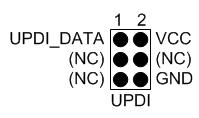
| MPLAB PICkit 5 Pin | Adapter Board AVR JTAG Pin | Legacy UPDI Pin | Name | Description |
|---|---|---|---|---|
| 1 | 7 or 8 (NC) | |||
| 2 | 4 (VDD/VTG) | 2 | VCC/VTG | Target voltage (reference voltage). |
| 3 | 2 or 10 (GND) | 6 | GND | Ground |
| 4 | 3 (TDO) | 1 | UPDI_DATA* | UPDI data. Other pin functions are possible depending on the device. |
| 5 | 1 (TCK) | |||
| 6 | 6 (MCLR) | |||
| 7 | 9 (TDI) | |||
| 8 | 5 (TMS) | |||
| * A High-Voltage (HV) pulse on this pin may be necessary to use the UPDI function. See your device data sheet for UPDI configuration. | ||||