1 SPI Slave Interface
The ATWINC1500 provides an SPI that can be used for control and for serial I/O of 802.11 data. The SPI Slave pins are mapped as shown in the following table. The RXD pin is the same as the Master Output, Slave Input (MOSI), and the TXD pin is the same as the Master Input, Slave Output (MISO). The SPI slave is a full-duplex, slave-synchronous serial interface that is available following a reset when pin 9 (SDIO_SPI_CFG) is tied to VDDIO.
| Pin Number | Pin Name | SPI Function |
|---|---|---|
| 9 | SPI_CFG | Must be tied to VDDIO |
| 16 | SPI_SSN | Active low slave select |
| 18 | SPI_SCK | Serial clock |
| 13 | SPI_RXD | Serial data receive (MOSI) |
| 17 | SPI_TXD | Serial data transmit (MISO) |
When the SPI is not selected (SSN is high), the SPI does not interfere with data transfers between the serial-master and other serial-slave devices. When the serial slave is not selected, its transmitted data output is buffered, resulting in a high impedance driver onto the serial master receive line.
The SPI slave interface responds to a protocol that allows an external host to read or write any register in the chipset, as well as, initiate DMA transfer.
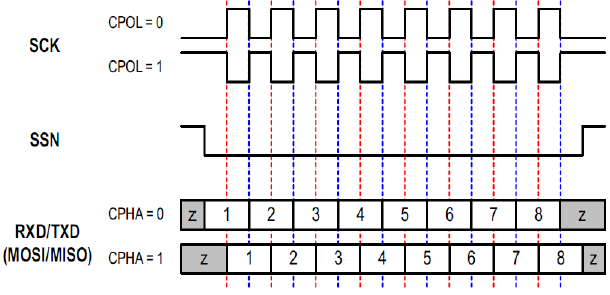
The SPI slave interface supports four standard modes as determined by the Clock Polarity (CPOL) and Clock Phase (CPHA) configuration. These modes are illustrated in the following table.
| Mode | CPOL | CPHA |
|---|---|---|
| 0 | 0 | 0 |
| 1 | 0 | 1 |
| 2 | 1 | 0 |
| 3 | 1 | 1 |
The red lines in the following figure correspond to Clock Phase = 0 and the blue lines correspond to Clock Phase = 1.