
4 Power Stage
The Multi-Phase Power Board power stage features four identical output channels. These are known as the board's “Phases” and are labeled A through D.
Each phase can be independently controlled through the adapter connector, and provides options for voltage and current feedback.
| Power Stage Performance | |
|---|---|
| Voltage Range | 6V to 50V |
| Power(1) | 10A at 24V |
Note: 1: Typical performance in base configuration. | |
4.1 Phase Output
Each output phase consists of two N-channel power MOSFETs (SIR120DP by Vishay) arranged in a half-bridge configuration. The gates are controlled by a Microchip MIC4605-1 half-bridge MOSFET driver, allowing individual control of the high and low side MOSFETs while providing shoot-through protection. The control signals are available through the adapter connector. Pull-down resistors are mounted close to the MIC4605, so neither MOSFET is active by default, causing the phase output to float. Each phase has a ten mΩ low-side current sense resistor routed into the on-board current sense system. | 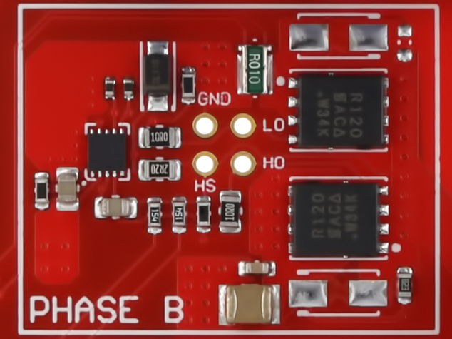 |

| SIR120DP Summary | |
|---|---|
| VDS | 80V |
| RDS(ON) max. at VGS= 10V | 0.00355Ω |
| Qg typ. | 48.5 nC |
| ID | 106A |
| Phase | Signal | Position on Adapter Connector |
|---|---|---|
| A | Drive A High | 26 |
| Drive A Low | 25 | |
| B | Drive B High | 24 |
| Drive B Low | 23 | |
| C | Drive C High | 22 |
| Drive C Low | 21 | |
| D | Drive D High | 20 |
| Drive D Low | 19 |
4.2 Voltage Feedback
The MPPB’s power stage provides voltage feedback options for each phase and includes a configurable virtual neutral point for back EMF measurements.
4.2.1 Phase Voltage Sense
The instantaneous output voltage of each phase is routed through a resistor divider before being exposed on the adapter connector. |  |
| Phase | Signal Name | Position on Adapter Connector |
|---|---|---|
| A | Feedback A | 12 |
| B | Feedback B | 10 |
| C | Feedback C | 8 |
| D | Feedback D | 6 |
4.2.2 Virtual Neutral Point
The 3-phase virtual neutral point is implemented using resistors and provides an instantaneous average voltage of the three phases connected to it. In the out-of-box configuration, phases A, B and C are connected to the virtual neutral. Other configurations are possible by modifying the board and moving the 0805-size 0-Ohm resistors. | 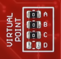 |

| Phase | Signal Name | Position on Adapter Connector |
|---|---|---|
| Virtual Neutral Point | Feedback N | 4 |
4.3 Phase Current Sense
The Multi-Phase Power Board features two independent current sense amplifiers, implemented using MCP6021op-amps in a differential summing configuration around a reference voltage.
The number of phases connected to each amplifier is configurable and will influence the transfer function as per Table 4-5.
| # Phases Connected | Amplifier Gain | Transfer Function |
|---|---|---|
| 1Ph | 15 | |
| 2Ph | 10 | |
| 3Ph | 7.5 |
4.3.1 Current Sense Amplifier 1
Current Sense Amplifier 1 can connect to phases A, B and C. In the out-of-box configuration, it is connected to all three. Other configurations are possible by modifying the board and moving the 0805-size 0-Ohm resistors. | 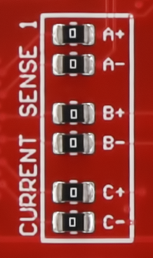 |

| Position on Adapter Connector | Silk Screen Marking |
|---|---|
| 7 | CS1 |
4.3.2 Current Sense Amplifier 2
Current Sense Amplifier 2 can connect to phases B, C and D. In the out-of-box configuration it is connected only to phase D. Other configurations are possible by modifying the board and moving the 0805-size 0-Ohm resistors. | 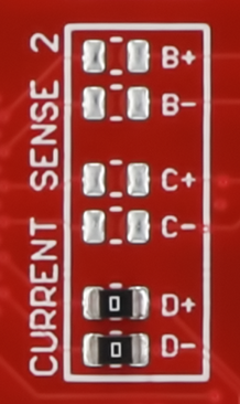 |

| Position on Adapter Connector | Silk Screen Marking |
|---|---|
| 5 | CS2 |
4.3.3 Voltage Reference
The voltage reference generates the midpoint voltage for the current sense amplifiers. It is implemented as a voltage divider feeding into an MCP6021 op-amp configured as a unity gain amplifier. The Vref circuit output is also available on the adapter connector as an ADC reference. |  |
| Position on Adapter Connector | Silk Screen Marking |
|---|---|
| 3 | VREF |