
3 Functional Description
The SY75712 and SY75714 are two- or four-output, ultra-low additive jitter, 1.2V to 1.8V LVCMOS fanout clock buffers with synchronous Output Enable (OE) control signal. The devices can operate at an extended temperature range from –40°C to +105°C.
The outputs have built-in 50Ω series resistance which makes them suitable for driving standard transmission lines (50Ω characteristic impedance) without any external components.
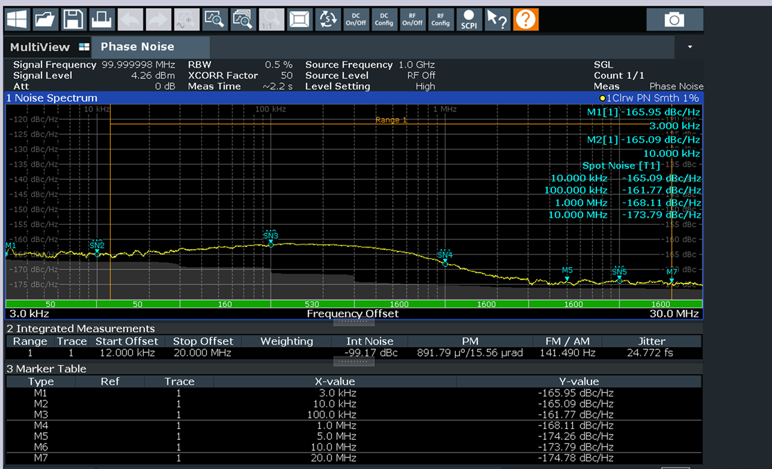
The following phase noise plots captured with an R&S FSWP8 Phase Noise Analyzer show typical phase noise performance. Figure 3-1 shows the phase noise of input clock generated with R&S SMA100B signal generator and Figure 3-2 shows the SY75712/14 output phase noise.
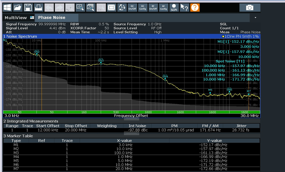
The plot in Figure 3-2 shows that the device has a very low noise floor of –171.7 dBc/Hz, which results in ultra-low additive jitter in the 12 kHz to 20 MHz band of only 15 fs.