
9 PCB Layout and Manufacturing Recommendations
When designing hardware that incorporates the Nano Debugger, it is essential to follow all recommended design practices for working with a SAMD21 device.
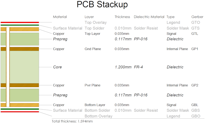
PCB Stackup
A 4-layer PCB is recommended, as it offers optimal noise decoupling and allows for precise control of trace impedances for USB signals. The standard 0.062" (1.594 mm) four-layer PCB stack-up, available from most PCB fabricators, is suitable for this purpose. This stack-up is used for all Curiosity Nano MCU boards.
An example of a PCB stack-up from a Curiosity Nano board is provided below.
USB Traces
The standard specification for USB 2.0 trace impedance is 90 ohms for differential pairs, which can be readily achieved on a 4-layer PCB. The USB interface pins on the SAMD21 are designed with the appropriate matching impedance, so no additional series termination resistors are needed between the USB connector and the Nano Debugger.