6 Example Applications
To show the advantages and disadvantages of using Power over Data Line on a mixing segment, a practical example with several PD nodes and a single PSE was created and tested. This mixing segment was then tested and measured once while PoDL was used, and once where the PoDL power supply circuit was missing on the PCBs. In this case, the cable to the PSE on the network was also removed. The topology used is shown in Figure 6-1.

The PSE consisted of a simple injector circuit which measured the injected voltage, current and total power. The power output was filtered by a pair of coupled inductors with a nominal inductance of 47 µH and a maximum current of 1.44A. The voltage injection of the PSE was measured at 11.50V with a voltage noise of 1.6 mV Root-Mean-Square(RMS) and 22.6 mV Peak-to-Peak(PkPk) when measured across a 47Ω resistor, providing 2.8W of power.
To measure the amount of noise on the mixing segment due to switching regulators and LDOs, a quick measurement was done while all devices were put into sleep mode. In this case, the PSE supplied a voltage of 11.55V at 2.0W with a RMS noise of 3.2 mV and a PkPk noise of 81.1 mV.
A similar measurement was done while all devices were active and powered. The PSE provided a voltage of 11.44V at 3.5W, with a RMS noise of 3.5 mV and PkPk noise of 78.3 mV.
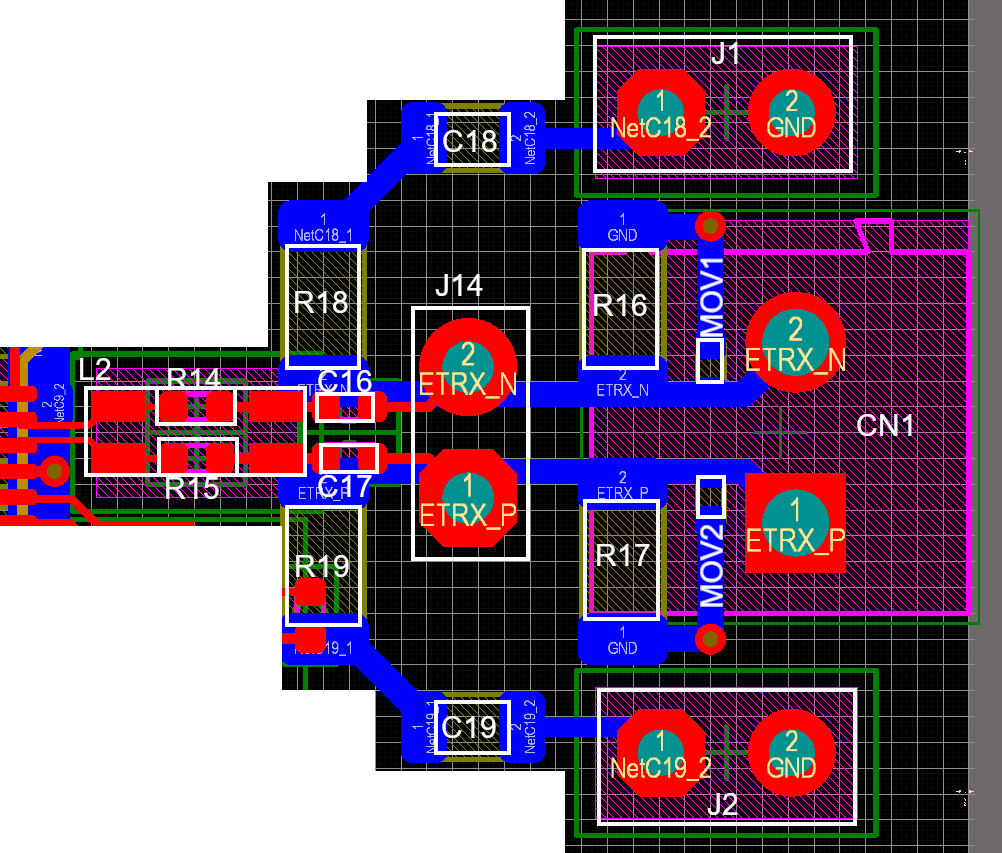
The PDs used the same hardware and only differed in their Node ID. The schematic of the BIN circuit is shown in Figure 6-2, while the layout of the BIN is shown in Figure 6-3. The jumpers J14, J15 and J16 are used to connect a separate add-on board containing the PoDL circuitry. Jumper J14 connects the T1S PoDL network to the input circuitry of the board, jumper J15 connects the 5V power supply level to the add-on board and jumper J16 connects the ground GND to the add-on board. The add-on board uses the PoDL supply to generate a 5V output, supplying the main board with power. When used, the add-on board provides power to the main board, when omitted the main board must be powered by an external power supply.
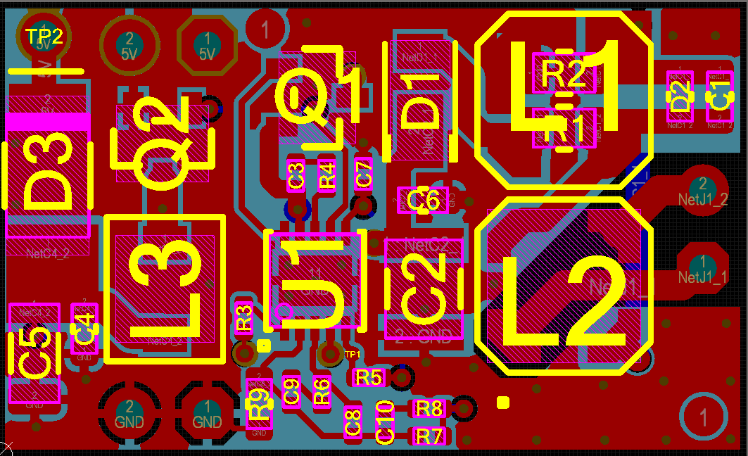
An add-on board was used to provide the PoDL circuit. The schematic of the add-on board is shown in Figure 6-4, while the corresponding layout is shown in Figure 6-5. Jumper J1 connects to a T1S network with PoDL. Jumper J2 is an 5V power supply output, powered by the PoDL network, while jumper J3 connects to the GND plane of the accompanying board. When connected to the main board from above, jumpers J1 must be connected to J14, J2 to J15, as well as J3 to J16.