
3.2.1.3.1 Steps to Configure the Application Modules
Create separate VS Code projects for the AVR128DA48 and PIC32CM6408PL10 microcontrollers. Open MCC and perform the following steps to configure the application modules.
Step 1: Clock Configuration
Step 2: Peripheral Configuration
Step 2.a: I2C Configuration
In this application, the temperature sensor (MCP9808) is connected through the I2C interface. The Two-Wire Serial Interface (TWI) peripheral on the AVR128DA48 and the SERCOM I2C peripheral on the PIC32CM6408PL10048 are configured with the settings below to read temperature sensor data. The sensor data read through the I2C interface is processed in the application code and displayed as temperature in degree Celsius.
Add the I2C module to the Project Resources and configure it for a 100 kHz communication speed. Use Figure 3-6 and Figure 3-7 as references for configuring the I2C peripheral on the AVR128DA48 microcontroller.
TWI Peripheral in AVR® DA
SERCOM I2C (SERCOM0) Peripheral in PIC32CM PL10
Add the SERCOM0 module to the project, configure it as I2C Master, and set the communication speed to 100 kHz. Use Figure 3-8 as a reference for configuring the I2C peripheral on the PIC32CM6408PL10048 microcontroller.
Step 2.b: ADC Configuration
The Curiosity Nano Explorer board includes a rotary potentiometer connected to one of the analog input channels of the ADC. The ADC periodically samples and converts the potentiometer signal. As the user rotates the potentiometer, the corresponding output voltage is sensed and measured by the ADC peripheral. Both the AVR128DA48 and PIC32CM6408PL10048 feature a 12-bit ADC.
Add the ADC peripheral to the Project Resources. Then, configure the module as shown in Figure 3-9 for the AVR128DA48 microcontroller.
Select VREF from Project Resource>Drivers and configure VDD as ADC Voltage Reference Source as shown in Figure 3-10.
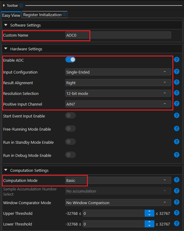
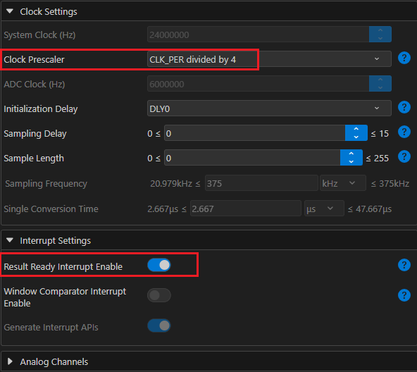
Similarly, for the PIC32CM6408PL10 microcontroller, add the ADC module to the Project Resources and configure it as shown in Figure 3-11.
Step 2.c: RTC Configuration
In this application, a Real-Time Counter (RTC) peripheral is used to periodically read the temperature sensor and the variable output voltage from the rotary potentiometer. By default, the RTC generates a compare interrupt every 500 ms and initiates the I2C transfer and an ADC conversion to read the temperature sensor and potentiometer values, respectively. With every switch press on the Curiosity Nano board, the RTC interrupt period changes to 1s, 2s, 4s, and then returns to the default 500 ms interval.
Add the RTC module to the Project Resources and configure it to generate a 500 ms interrupt, as shown in Figure 3-12 for the AVR128DA48 microcontroller.
Similarly, for the PIC32CM6408PL10 microcontroller, add the RTC module to the Project Resources and configure it as shown in Figure 3-13.
Step 2.d: Configuring the Port Pin for Switch
The AVR® DA and PIC32CM-PL10 Curiosity Nano boards have on-board switches. The AVR® DA device detects switch presses using the interrupt capability on port pins, whereas the PIC32CM PL10 device uses an External Interrupt Controller (EIC) peripheral. The EIC allows external pins to be configured as interrupt lines and can generate interrupts on rising, falling or both edges. In this application, the EIC is configured to detect a falling edge on the pin connected to the on‑board switch. Refer to Figure 3-14 to configure PB03 as a switch input. Refer to Step 3: GPIO/Port Configuration to see how the port pin is configured on the AVR128DA48.
Step 2.e: Timer Configuration
Since the on‑board switch is used to change the RTC interrupt periodicity, the application must handle switch debouncing. To achieve this, a timer peripheral is used to generate a 50 ms overflow interrupt upon detecting a falling edge on the switch pin. The Timer/Counter Type A (TCA) peripheral is configured on the AVR128DA48, and the Timer/Counter0 (TC0) peripheral on the PIC32CM6408PL10048 to manage switch debouncing.
For the AVR128DA48 microcontroller, add the TCA0 peripheral to the Project Resources and configure it as shown in Figure 3-15.
Similarly, for the PIC32CM6408PL10 microcontroller, add the TC0 peripheral to the Project Resources and configure it as shown in Figure 3-16.
Step 2.f: UART Configuration
Configure the Universal Asynchronous Receiver and Transmitter (UART) peripheral to periodically print the temperature sensor and ADC results to the terminal. The AVR DA requires configuration of both the UART driver and PLIB instances.
For the AVR128DA48 microcontroller, add the UART peripheral to the Project Resources and configure it for a baud rate of 115200, as shown in Figure 3-17.
Enable the USART Receiver and Transmitter interrupts from the UART PLIB configuration, as shown in Figure 3-18.
Similarly, for the PIC32CM6408PL10 microcontroller, add the SERCOM1 peripheral to the Project Resources and configure it for a baud rate of 115200, as shown in Figure 3-19.
Add STDIO from Device Resources>Libraries>Harmony>Tools and connect its corresponding UART to the SERCOM1 UART, as shown below.
Step 3: Port Configuration
After configuring the peripherals, configure the pin setting as shown below. On the AVR128DA48, the port pin connected to the on-board switch is configured through Pin settings to detect a falling edge and generate an interrupt.
For the AVR128DA48 microcontroller, open the Pin Grid View in MCC and configure the pin assignments according to Figure 3-21: USART1 (TXD - RC0), TWI0 (SDA - PC2, SCL - PC3), ADC0 (PD7), GPIO Input (PC7), and GPIO Output (PC6).
For the AVR128DA48 microcontroller, open the Pins View in MCC and configure the switch interrupt on pin PC7 to detect a falling edge, as shown in Figure 3-22.
Step 4: Interrupt Settings
For the AVR128DA48 microcontroller, open the Interrupt Manager in MCC and toggle on Global Interrupt Enable.
For the PIC32CM6408PL10 microcontroller, go to Project Resources>System>Interrupts (NVIC) and enable the RTC, EIC, SERCOM0, TC0 and ADC0 interrupts.
Step 5: Generate Source Files
After configuring all peripherals, click the Generate button in the MCC window to generate the driver files. Refer to the Code Generation section for more details on MCC-generated files.
As the final step, add the application code to the AVR128DA48 and PIC32CM6408PL10048 microcontroller projects. The application code required for this example is available at the following link.