57.13.1.13.2 Timing Extraction
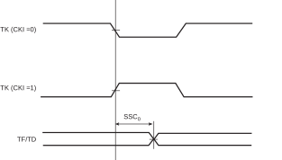
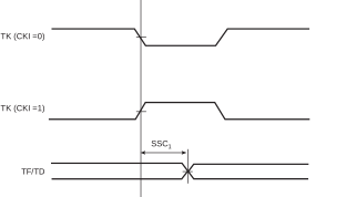
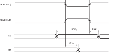
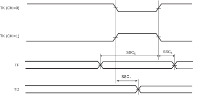
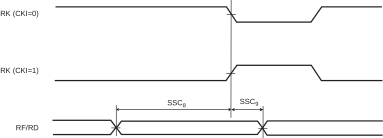
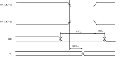
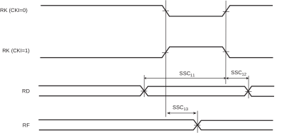
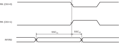
| Symbol | Parameter | Condition | Min. | Max. | Unit |
|---|---|---|---|---|---|
| Transmitter | |||||
| SSC0 | TK edge to TF/TD (TK output, TF output) | – | -3.9(1) | 4.0 (1) | ns |
| SSC1 | TK edge to TF/TD (TK input, TF output) | – | 3.1(1) | 12.7(1) | ns |
| SSC2 | TF setup time before TK edge (TK output) | – | 13.6 | – | ns |
| SSC3 | TF hold time after TK edge (TK output) | – | 0 | – | ns |
| SSC4 | TK edge to TF/TD (TK output, TF input) | – | -3.9(1) | 3.0(1) | ns |
| STTDLY = 0 START = 4, 5 or 7 | -3.9 + (2× tCPMCK)(1) | 3.0 + (2 × tCPMCK)(1) | |||
| SSC5 | TF setup time before TK edge (TK input) | – | 0 | – | ns |
| SSC6 | TF hold time after TK edge (TK input) | – | tCPMCK | – | ns |
| SSC7 | TK edge to TF/TD (TK input, TF input) | – | 3.1(1) | 11.8(1) | ns |
| STTDLY = 0 START = 4, 5 or 7 | 3.1 + (3 × tCPMCK)(1) | 11.8 + (3 × tCPMCK)(1) | |||
| Receiver | |||||
| SSC8 | RF/RD setup time before RK edge (RK input) | – | 0 | – | ns |
| SSC9 | RF/RD hold time after RK edge (RK input) | – | tCPMCK | – | ns |
| SSC10 | RK edge to RF (RK input) | – | 2.9(1) | 9.2(1) | ns |
| SSC11 | RF/RD setup time before RK edge (RK output) | – | 10.1 - tCPMCK | – | ns |
| SSC12 | RF/RD hold time after RK edge (RK output) | – | tCPMCK - 2.8 | – | ns |
| SSC13 | RK edge to RF (RK output) | – | -2.1(1) | 1.9(1) | ns |
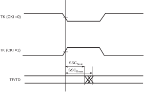
Note: For output signals (TF, TD, RF), minimum
and maximum access times are defined. The minimum access time is the time between the TK
(or RK) edge and the signal change. The maximum access timing is the time between the TK
edge and the signal stabilization. The figure below illustrates the minimum and maximum
accesses for SSC0, and the same is applicable for SSC1, SSC4, SSC7, SSC10, and
SSC13.