
5.5 Printed Circuit Board for 800V-12V 2700W PSFB-CDR
The use of 4 kV Isolated PSFB-CDR topology with a maximum of 180A output creates two zones in the physical implementation and design of PCB for this DC-DC converter. The input side is a high-voltage side with up to 1000V input voltage. The required current at 800V nominal input voltage for 2700W peak power becomes small with peak currents < 15A. The output side is low voltage with peak voltage spikes of < 100V but current demand increases up to a maximum of 180A output. Peak currents in the system may go up to 230A.
Additionally, due to high switching losses at primary Phase-Shifted Full-Bridge and high conduction losses at secondary Synchronous MOSFETs, heat generated must be effectively taken out of the system to maintain a safe operating junction temperature for the silicon devices. This is done through use of copper coin technology or copper embeds, which provide a low thermal resistance from MOSFET pads to the heat sink below, by means of a thermal interface material.
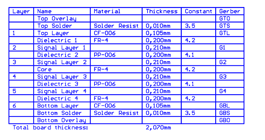
The printed circuit board is made up of 6 Cu-layers. Figure 5-7 shows layer stack-up.
The minimum clearance requirement for this PCB is derived from high-voltage isolation requirements and minimum possible feature size which comes from manufacturer capabilities for fabricating 105 um and 210 um Cu-Layers.
| Zones / Net Class | Clearance | Layer | Comments |
|---|---|---|---|
|
HV to HV |
3mm for 1kV |
External |
Between two high-voltage side objects |
|
HV to HV |
1.5mm for 1kV |
Internal |
Internal layer clearance requirements are less as compared to the outer layer. |
|
HV to LV |
6mm for 4kV |
External |
HV to LV clearance ties directly with safe of the system hence a minimum of 6mm is selected. |
|
HV to LV |
3mm for 4kV |
Internal |
Internal layer clearance is smaller as compared to the outer layer. |
|
LV to LV |
0.25mm |
External |
0.25mm works well for voltage < 100V. It is the minimum clearance needed for 105um Cu Layer thickness. |
|
LV to LV |
0.5mm |
Internal |
0.5mm minimum clearance is needed for 210um Cu Layer thickness. |
Table 5-2 is used for sizing secondary side high-current internal and external layer Cu traces.
| Proposed Current density | Comments |
|---|---|
| IPC-2221A and IPC-2152 | As per standards, proposed current density for a 10⁰C temperature rise is as following, Outer layers= 38A/mm2 , Inner layers= 19A/mm2. |
Considered for this design | In this design, inner and outer layer current density was selected as 8A/mm2. |