5.1 Creating a Bootloader Client
This example shows how to configure a bootloader for 8-bit PIC and AVR devices using UART
or SPI for communication.
Description: This section details a full standard bootloader use case on the PIC18F57Q43 microcontroller, which applies to many variants of the PIC18F family and can also be extrapolated to other 8-bit PIC and AVR chips as well. This example uses the PIC18F57Q43 Curiosity Nano board for demonstration. Refer to the board schematics for configuration information.
When using SPI communication, the target device can be connected to the PC through the MCP2210 Breakout Module for USB-to-SPI conversion.
Example: See how to bootload a program that blinks the LED of a PIC microcontroller.
-
Create a new MPLAB X IDE project.
Figure 5-1. New Project 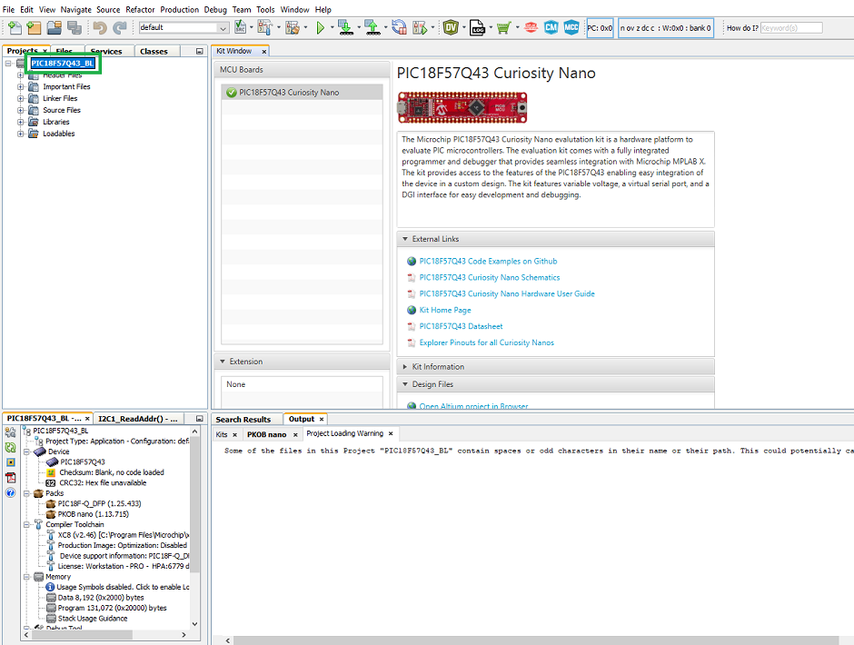 Note: If only “Simulator” is displayed in the Tools combo box while selecting the device, then the target board is not plugged into the computer or it is not communicating with MPLAB X IDE properly.
 -
MCC opens up automatically when a new project is created. If not, click the MCC button in the menu bar to start the MPLAB Code Configurator.
Figure 5-2. Open MCC 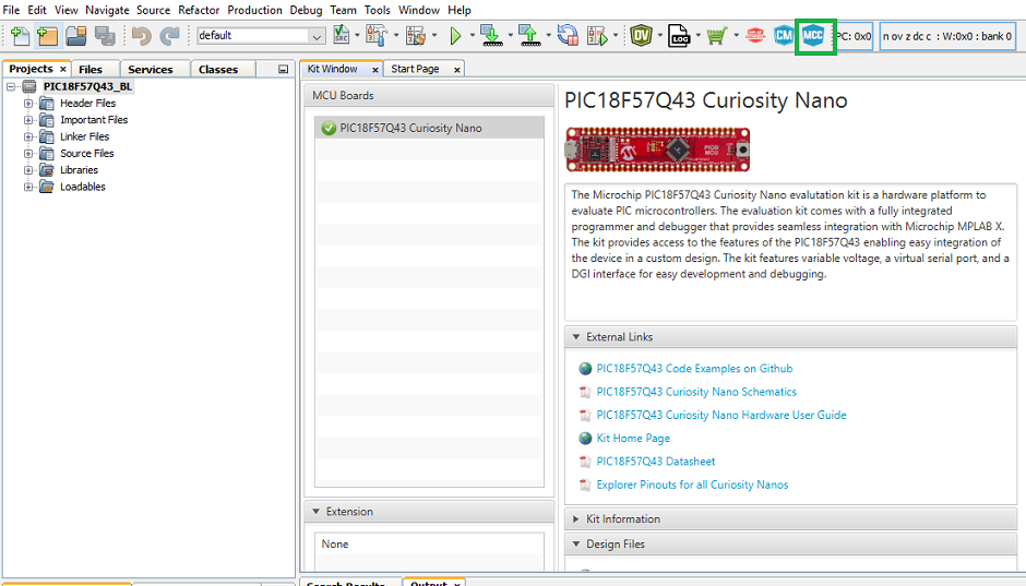
-
Click Next on MCC Melody in the MCC Content Type Wizard window.
Figure 5-3. Select MCC Melody 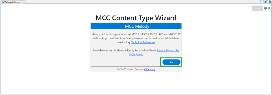
-
Click Finish once all the required content is downloaded in the Content Download Required window.
Figure 5-4. Content Download 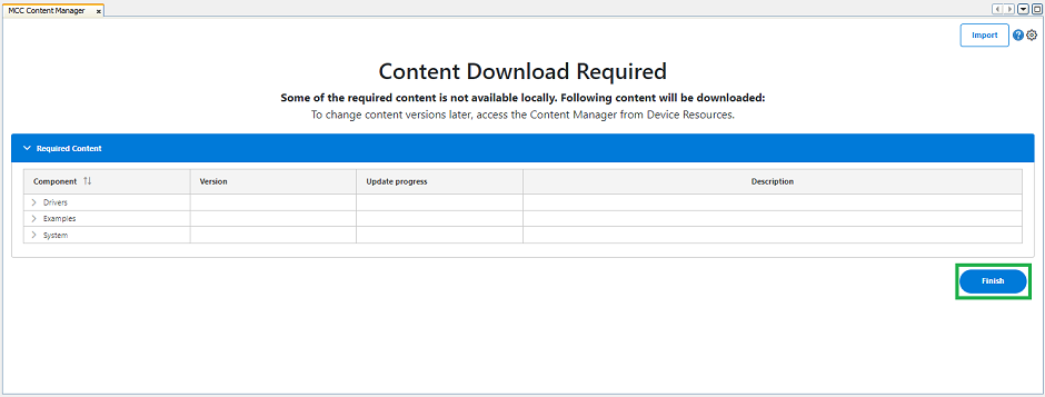
- Open the MCC Content Manager from
the Device Resources tab and make sure the latest version of 8-Bit MDFU Client is
downloaded under Libraries>Bootloader.
Figure 5-5. MCC Content Manager 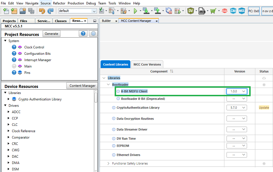
-
Bring the 8-Bit MDFU Client library into the Project Resources tab from Device Resources. In previous versions of MCC, a user needed to manually attach all peripheral drivers required by their library, using the Device Resources tab. The new MCC Melody allows users to select the library needed for the project from Device Resources. Melody brings in all the dependencies and configures them.
Figure 5-6. Device Resources 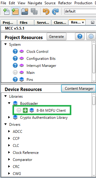
-
Confirm that the 8-Bit MDFU Client library has been included into the Builder window. Builder UI reflects all the required peripheral driver dependencies such as the Memory or NVM and Timer Delay modules and links them to the 8-Bit MDFU Client library.
Figure 5-7. Builder UI 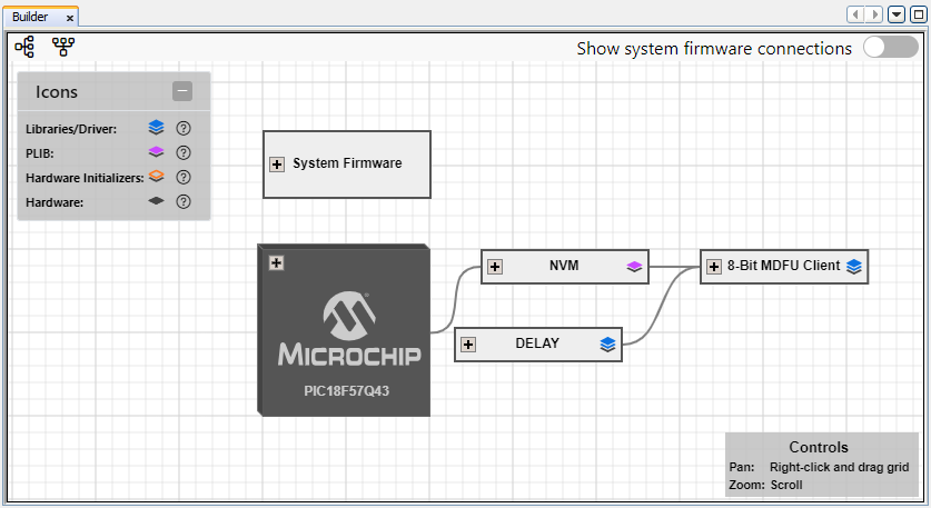
One of the modules that cannot be configured automatically is the communication peripheral.
UART:
Select UART from the Communication Protocol drop-down list in the 8-Bit MDFU Client Easy View tab.
Figure 5-8. UART Communication Protocol 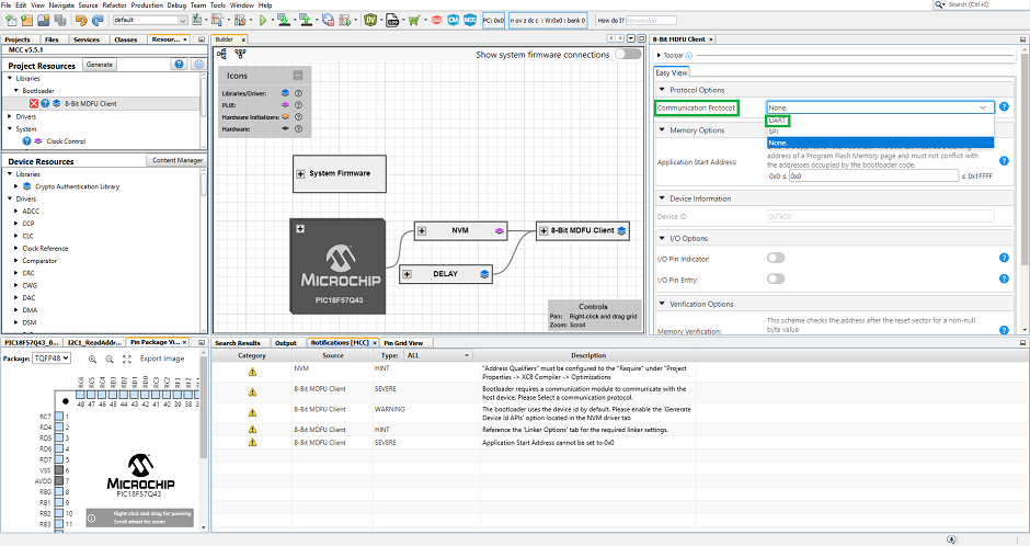
For the bootloader to communicate with the Bootloader Host Application, a communication driver needs to be exposed to exchange data through the serial ports on the target device. To understand which communication ports are required to be opened for the device in use, check the schematics and look for the Serial or CDC Ports definition for the Curiosity Nano board, as shown in the image below. Using this definition, the MCU is communicating through the RF0 pin for transmitting data serially and the RF1 pin for receiving data serially.
Note: Similarly, the SPI driver can be configured following the device schematics or data sheet for pin information.Figure 5-9. Serial/CDC Port 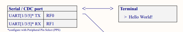
A communication driver version that communicates through the RF0 and RF1 pins is needed. For workflows on the PIC18F57Q43 Curiosity Nano, attach the UART1 driver, as that is the UART driver that can communicate through those pins. Select UART1 from the “UART PLIB Selector” in the UART(None) tab. The UART1 settings will open up.
Figure 5-10. UART PLIB Selector 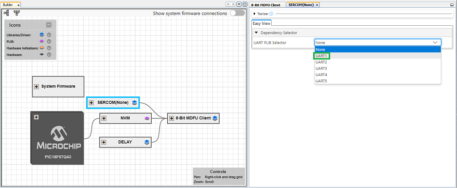
Figure 5-11. UART1 Settings 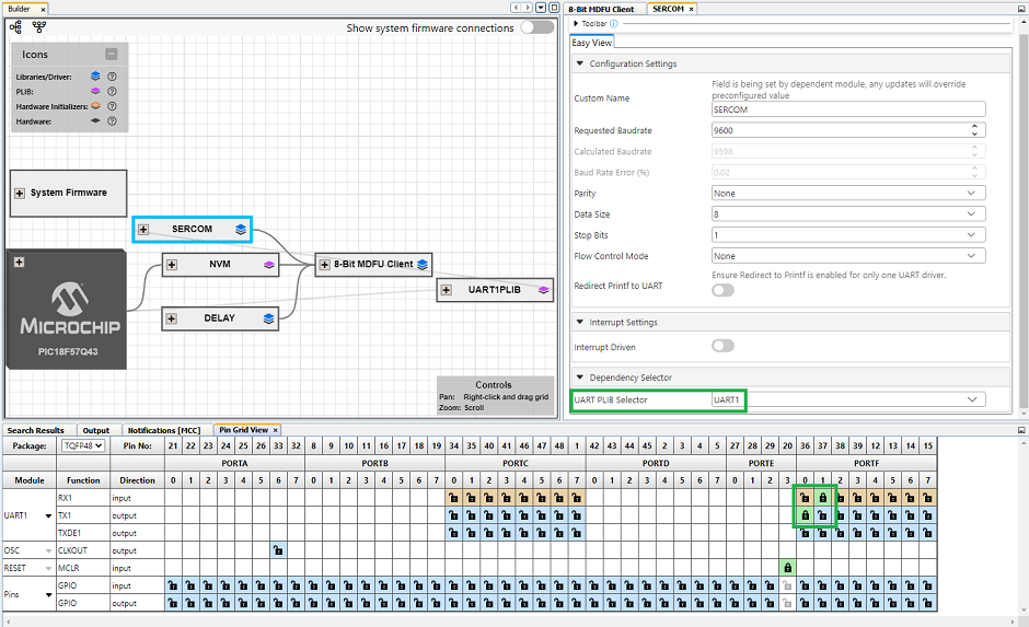 Note: Some devices will automatically select the required UART pins. Open the Pin Grid View tab to make sure the pins are enabled.
SPI:
Select SPI from the Communication Protocol drop-down list in the 8-Bit MDFU Client Easy View tab.
Figure 5-12. SPI Communication Protocol 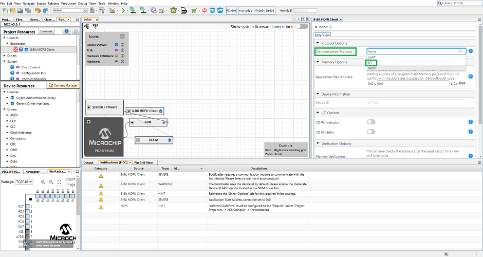
Select an instance of the SPI driver from the SPI Client PLIB Selector drop-down list. For example, SPI1 and the driver settings will open up.
Figure 5-13. SPI Client PLIB Selector 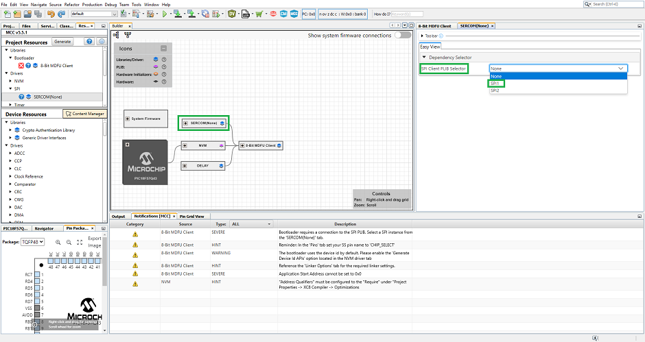
Make sure the correct SDI, SDO, SS and SCK pins are selected and rename the SS pin to CHIP_SELECT.
Figure 5-14. SPI Settings 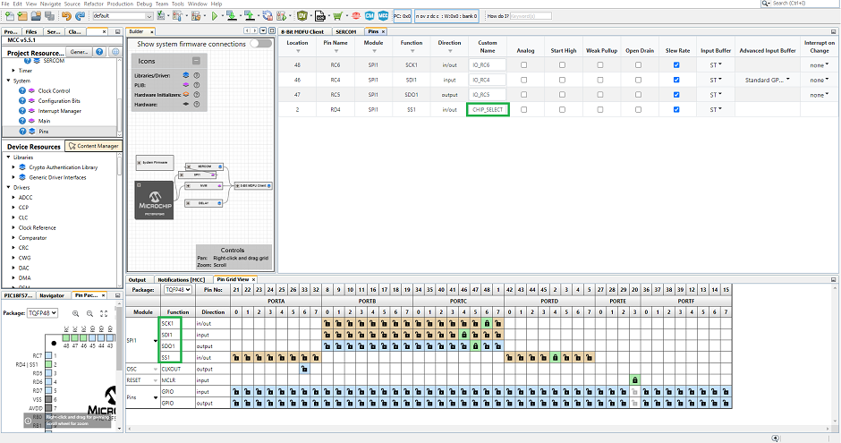
- In the System/Clock Control module,
configure the oscillator and clock divider. In general, faster clock is better for more
reliable communication. For this PIC18F57Q43 example, 64 MHz internal oscillator is selected
with Clock Divider set to 1.
Figure 5-15. Clock Control Settings 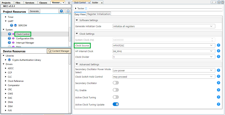
- For PIC devices, in the
System/Configuration Bits module, set the External Oscillator Selection to “Oscillator not
enabled”. Note: Make sure to match the clock settings and configuration bits settings in the bootloader client and the end application.
Figure 5-16. PIC® Configuration Bits Settings 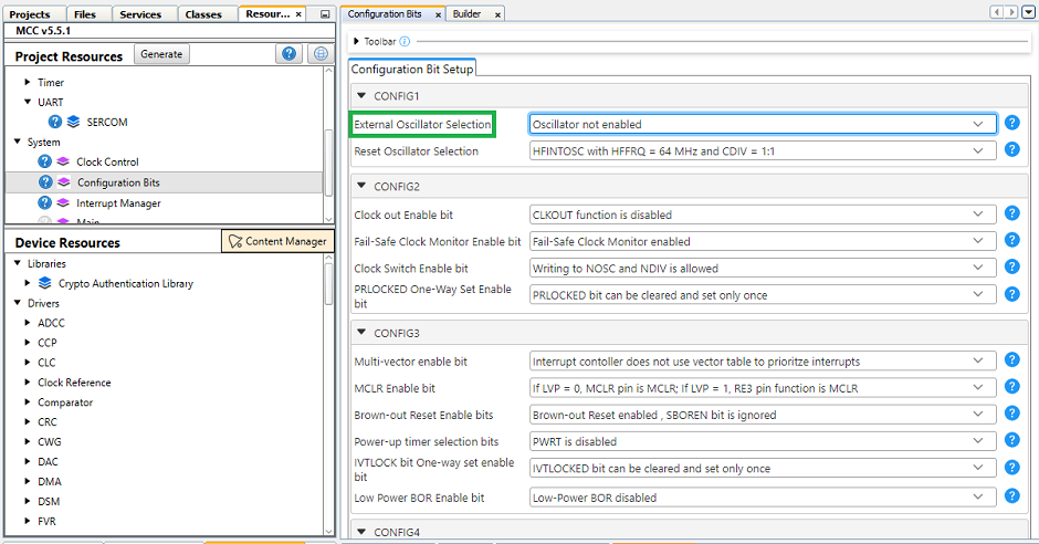
-
There are several advantages of configuring I/O pins, but the most important one is receiving a state back from the MCU based on the LED status. For example, the bootloader module will light up the LED when in a Boot state, and it will turn off when the application state takes over. This helps to track the program flow during the development process.
Configuring the bootloader module to utilize the I/O Indicator pin sets up the functionality. This is done by clicking the switch that activates the I/O Pin Indicator. The I/O Entry pin can also be configured to force the MCU into a Boot state by checking for voltage levels on the entry pin at any device Reset. To activate this pin, select the I/O Pin Entry switch from the 8-Bit MDFU Client tab.
Figure 5-17. I/O Pins 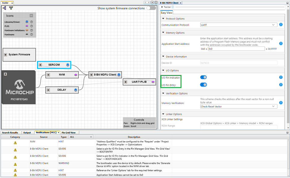
Check the schematics to configure the I/O pins for using the LED and switch on the board. Find the I/O interface declaration, similar to the image below. For the PIC18F57Q43, make sure the RF3 port is connected to control the LED and RB4 is connected to control the switch.
Figure 5-18. On-Board Peripherals 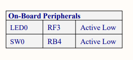
Go back to MPLAB X IDE and navigate to the Pin Grid View tab in the bottom center of the screen. Then select the RF3 and RB4 pins for BOOT INDICATE and BOOT ENTRY in the grid, respectively.
Figure 5-19. Pin Grid View 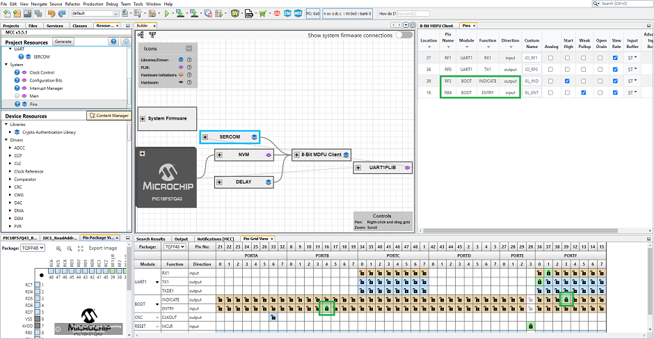 Note: For further configuration, access the Pins Module UI through Project Resources> System>Pins. Also refer to the device data sheet for pin pull-up/pull-down requirements.
 - Device ID is automatically populated for
the device used in the current project.
Figure 5-20. Device Information 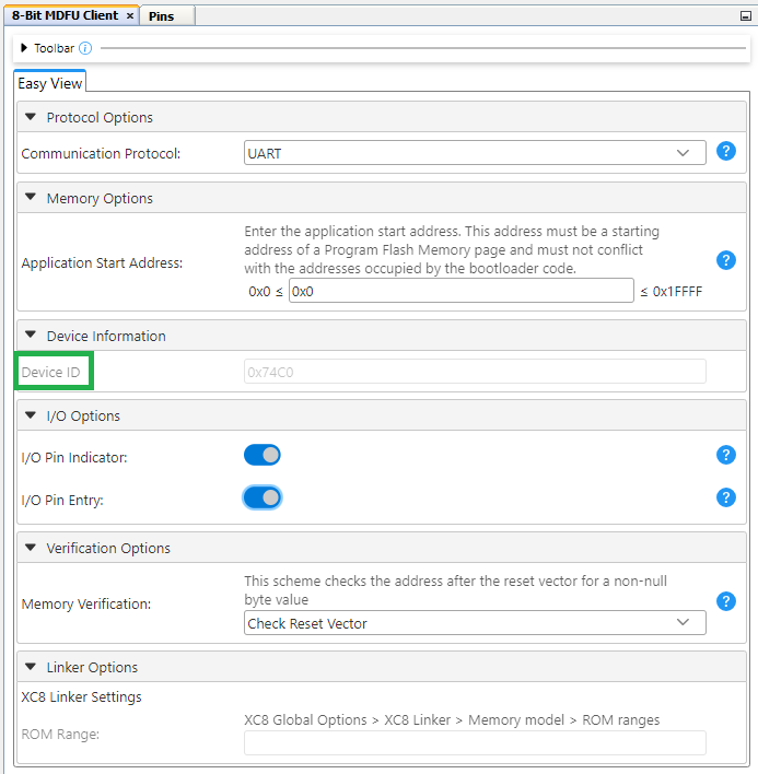
-
Before generating the initial code, address the warnings in the Notifications [MCC] tab. For example, NVM options must be enabled.
Figure 5-21. Notification [MCC] Tab 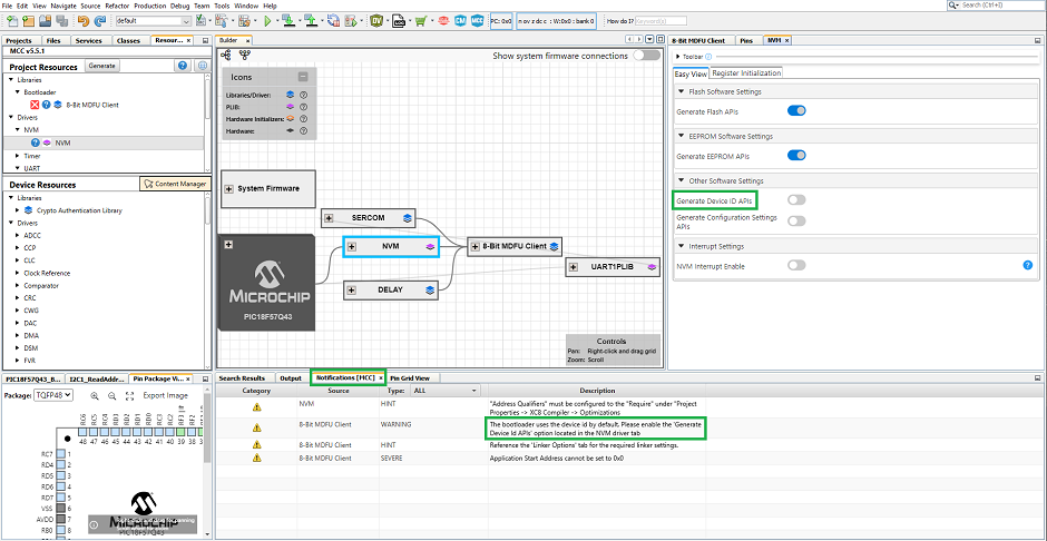
For example, enable Generate Device ID APIs for the NVM driver. Addressing the notification will either turn it into a hint or remove it from the list.
Figure 5-22. Clear NVM Notification 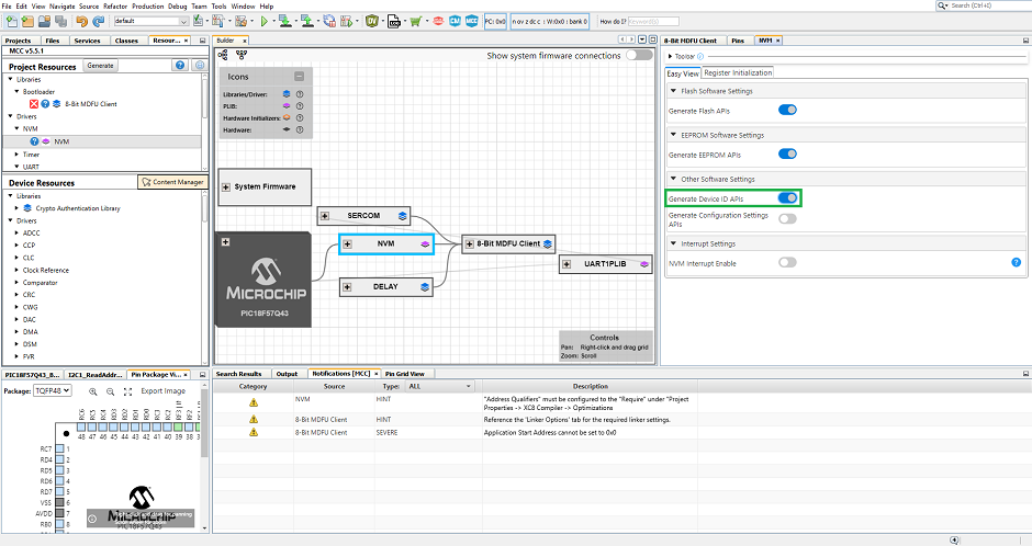
For the notification “Application Start Address cannot be set to 0x0”, set the memory offset/Application start address to the program memory size. The actual value of the application start address can be calculated after compiling the project for the first time.
Note: Initially, the Application Start Address is set to the end of the Flash address. This value will be scaled to the correct address after compilation.PIC:
Figure 5-23. Application Start Address 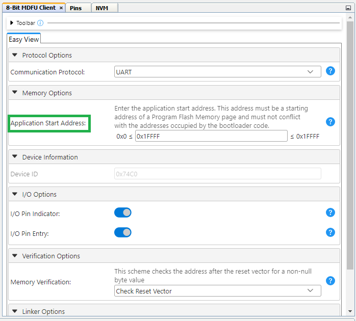
AVR:
For AVR devices, set BOOTSIZE in the Configurations Bits section to the maximum size - 1. For example, AVR128DA48 has a total of 256 pages (range is 0 to 255). Set the value to 254. The remaining one page is for the application image. The actual value of the BOOTSIZE can be calculated after compiling the project for the first time.Figure 5-24. AVR® BOOTSIZE - Configuration Bits 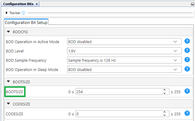
Figure 5-25. AVR® - Application Start Address 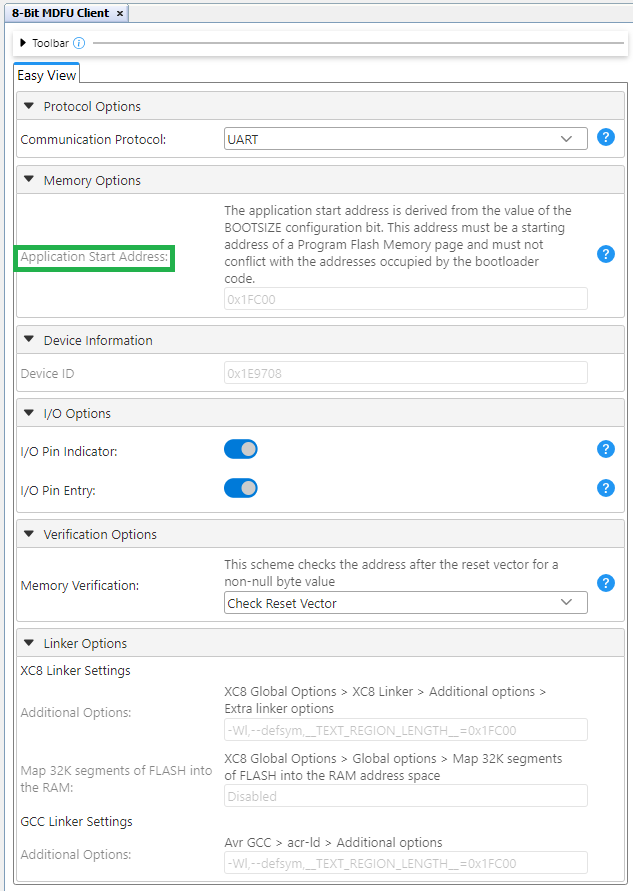
- For this example, the verification scheme
is set to Checksum.
Figure 5-26. Verification Scheme 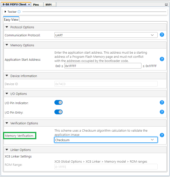
-
Now with the basic configurations complete, click the Generate button in the Project Resources tab to generate the project code.
Figure 5-27. Generate Project Code 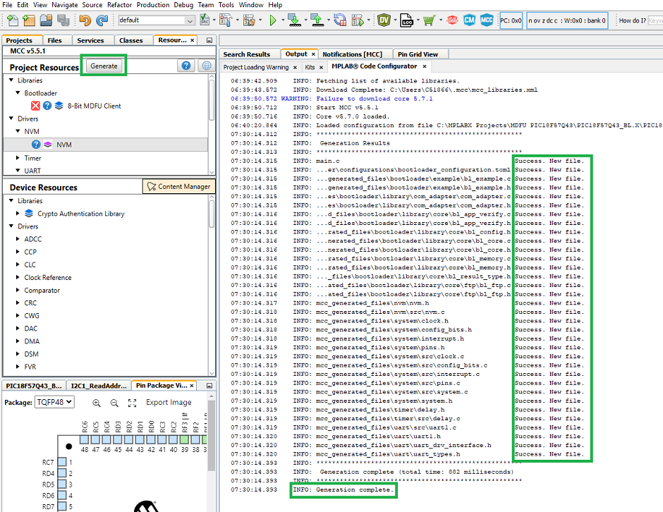
- The
bl_example.cfile provides API routines for running a bootloader update process. CallBL_ExampleInitialize()andBL_Example()in themain.cfile, as shown below.Figure 5-28. Bootloader Update Process Call 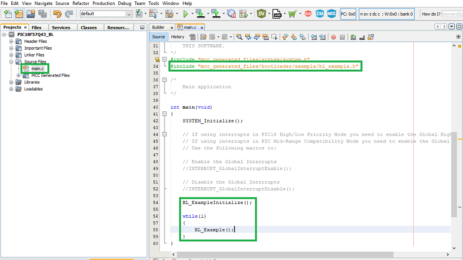
-
Click the “Clean and Build” icon drop-down option and select Clean and Build Main Project to compile the bootloader code.
Figure 5-29. Clean and Build Main Project 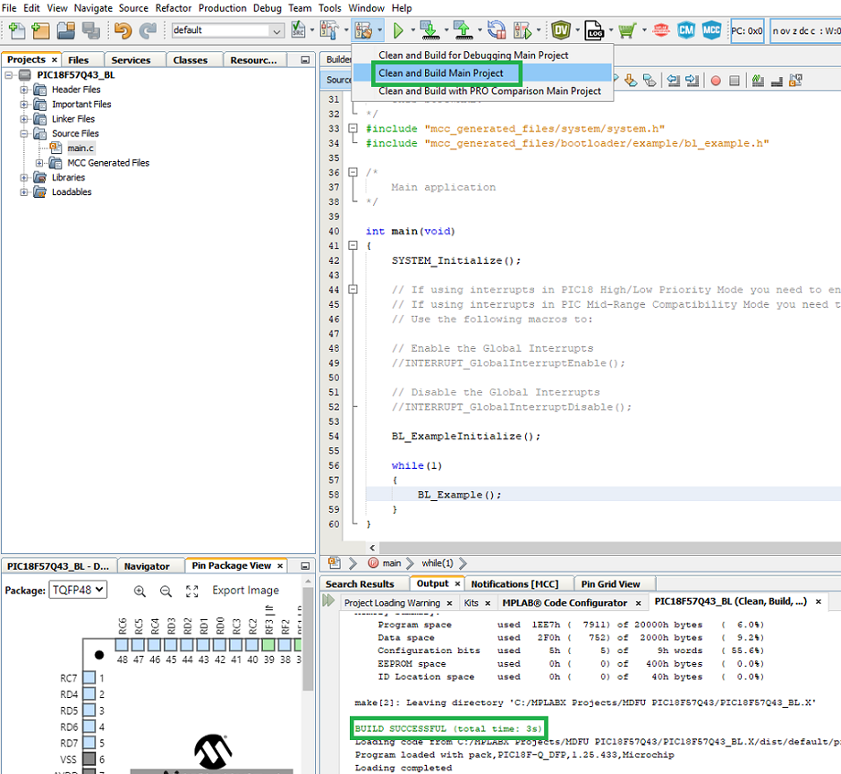
- The compilation log can be used to
determine the Program Space memory used by the project and the Application Start Address can
be set accordingly.
PIC:
The compilation log shows that the program space used is 1EE7h bytes. Update the Application Start Address to 2000h (starting address of the next page). Make sure to allocate enough space to account for Program Flash needed during operation.Figure 5-30. PIC® - Program Memory Consumption 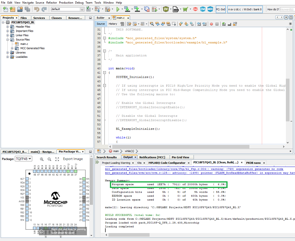
Figure 5-31. Updated Application Start Address 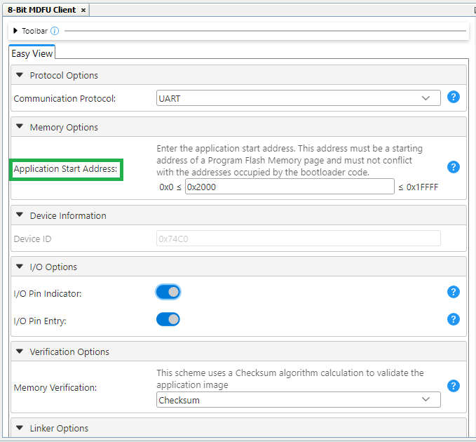
AVR:
With the device programmed, the next step is to calculate the FUSE size. As seen in the image below, the bootloader code is taking up memory from 0x0 to 0x123B. The Boot section of memory needs to be configured at a minimum 0x2000 bytes. The range must be pushed slightly higher to account for the RAM needed during operation. In this example, extra space is added to the bootloader to mimic a production design choice suitable for several solutions. There can also be a design where extra space is added to the Boot section to house an internal library within the Boot section of Flash.Figure 5-32. AVR® - Program Memory Consumption 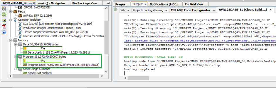 Note: Adding extra space in the Boot section of Flash is a design decision that must be considered on an as-needed basis.
The device used in this example, AVR128DA48, has the Flash memory divided into 100h pages with each page consisting of 200h bytes. Allocating 10h pages should provide the bootloader section with 2000h bytes (10h pages x 200h bytes) of Program Flash Memory and the remaining 0x1E000 for the user application.
Now set the FUSE values in the bootloader. Take the the BOOTSIZE Fuse calculated in the last step and plug it into the BOOTSIZE field within the Configuration Bits tab in the Project Resources.Note: Refer to the Memory Organization section of the device data sheet for more information on memory partition.Note: The “BOOTSIZE” field in the Configuration Bit Setup uses decimal values. Make sure to convert the calculated hex value to decimal value.Setting the CODESIZE fuse is an optional action that can be done in instances where a user wants more control over the various portions of memory. If this value is set to 0x00, the bootloader will still operate normally, but it is not possible to specify an AppData section of memory without first configuring the Codesize fuse. Refer to the memory map presented in the data sheet on how to configure this option.Figure 5-33. AVR® BOOTSIZE - Configuration Bits 
Figure 5-34. AVR® - 8-Bit MDFU Client Memory Options  Note: The “CODESIZE” field in the Configuration Bit Setup uses decimal values. Make sure to convert the calculated hex value to decimal value.
 - Before generating the code again and
programming the device, the linker settings have to be configured.
PIC:
Copy the ROM Range under Linker Option>XC8 Linker Setting. Right click the project and open project properties. Go to XC8 Global Option>XC8 Linker>Memory Model>ROM ranges and apply the copied value.Figure 5-35. 8-Bit MDFU Client - ROM Range - PIC® 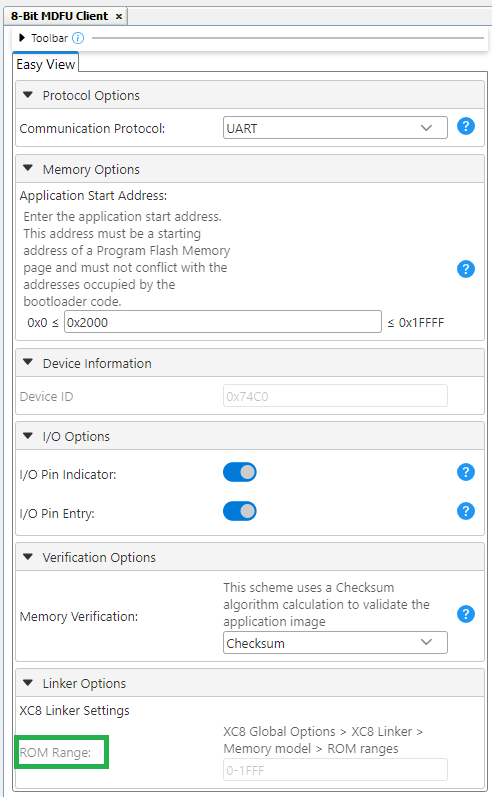
Figure 5-36. Compiler - Linker Settings - PIC® 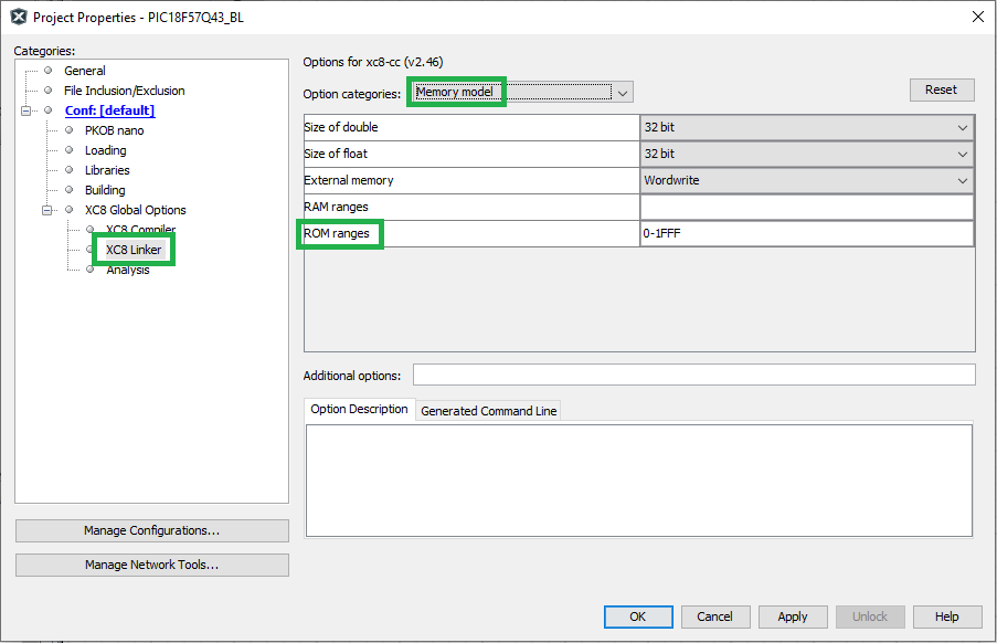
AVR:
Copy the Additional Options under the Linker Option>XC8 Linker Settings. Right click the project and open project properties. Go to XC8 Global Options>XC8 Linker>Additional Options>Extra Linker Options and apply the copied value.
Note: Make sure to uncheck “Map 32K segments of FLASH into the RAM address space” under the Project Project>XC8 Global Options>Global Options, if available, to prevent const data being written into Flash memory.Figure 5-37. 8-Bit MDFU Client - Additional Options - AVR® 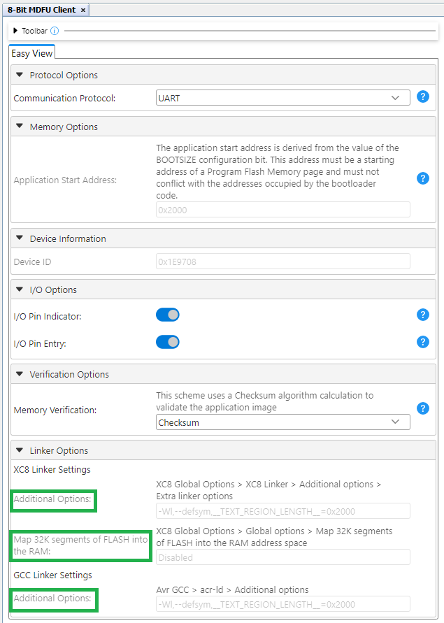
Figure 5-38. Complier - Linker Settings - AVR® 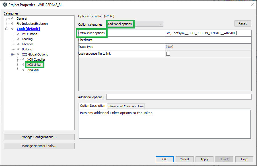
- Click the Generate button in the
Project Resources tab to generate the project code and compile the project again
with the updated Application Start Address.
Figure 5-39. Compile Project 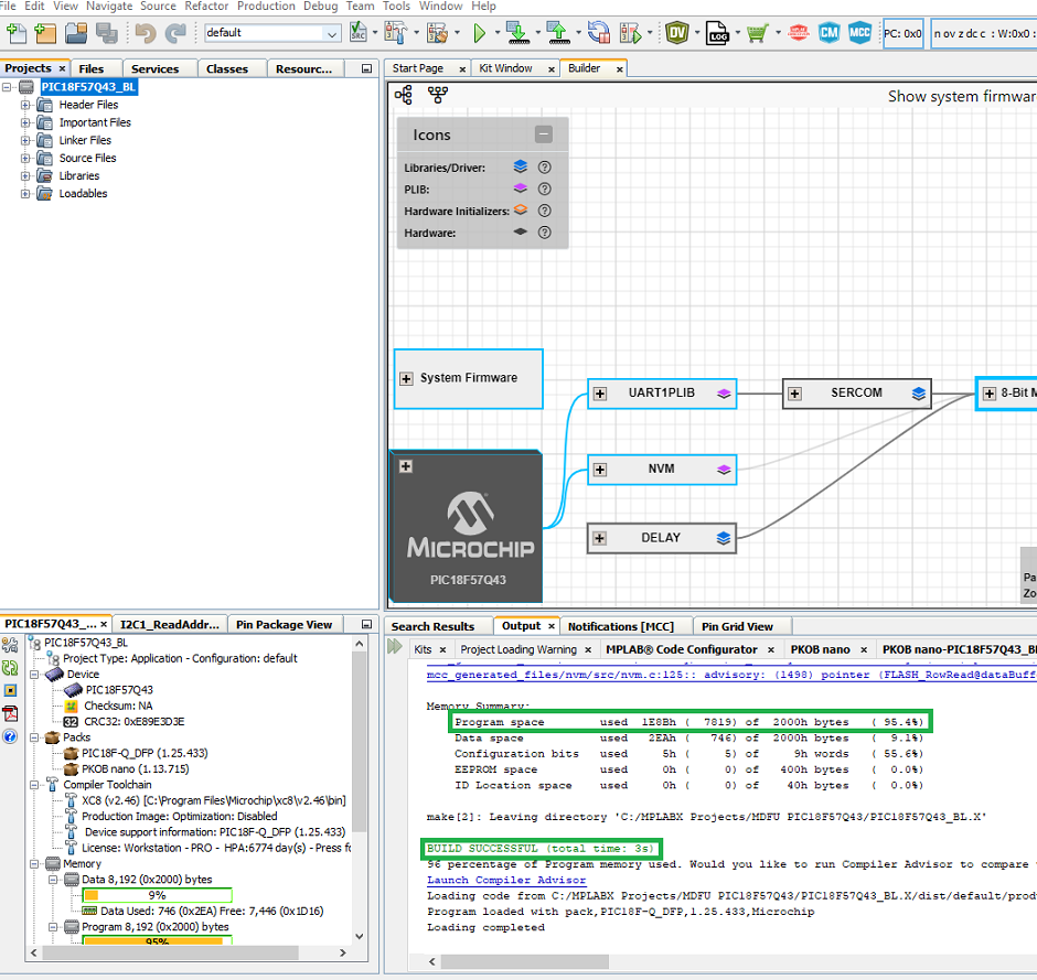
-
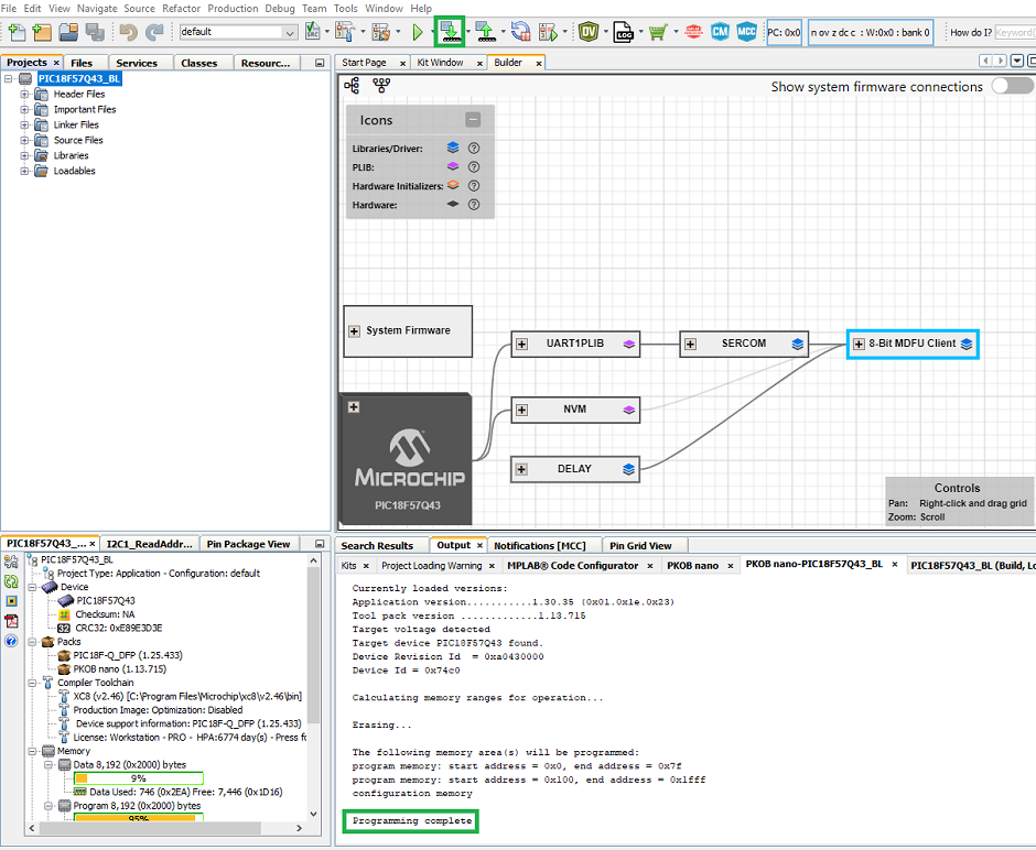
To prepare the chip to bootload, click the Make and Program Device button. After this programming process ends, the LED on the PIC18F57Q43 Curiosity Nano board will stay ON continuously.
Figure 5-40. Make and Program Device Main Project