
1.10 Getting Started with CLC
1.10.1 Introduction
| Author: Gheorghe Turcan, Microchip Technology Inc. |
Using logic gates, systems can make decisions based on criteria without Central Processing Unit (CPU) intervention. Traditionally, these logic gates are manually implemented as external components. However, the PIC® microcontrollers (MCUs) offer this as a built-in functionality.
The Configurable Logic Cell (CLC) has a variety of basic gates, as well as sequential logic options that can be customized to create the logic specific to many applications. Using these logic gates, the CLC gives the ability of combining signals to make a new custom signal without running code to execute it. The CLC also offers flexible input selection (internal, external signals) and configurable output for internal or external use with the help of the Peripheral Pin Select (PPS).
This technical brief explains the concepts of the CLC and its implementation in the PIC18 family of microcontrollers with the following use cases:
- Using Basic
Logic Gates:
This example shows how to use the CLC to implement the basic logic functions AND, OR and XOR of two internally generated signals. The outputs of the CLCs are connected to I/O pins.
- Using CLCs to
Create a Data Signal Modulator:
This example shows how to use the CLC in both J-K flip-flop and AND-OR configurations to obtain a DSM function (multiple frequency carrier signal).
- Using the CLC
to Create an LED Dimming Effect:
This example shows how to use the CLC in an SR Latch configuration to obtain a PWM signal that changes duty cycle without code addition. The change in duty cycle can be used to generate the effect of an LED dimming or increasing brightness instead of blinking.

1.10.2 Peripheral Overview
The Configurable Logic Cell (CLC) module provides programmable logic that operates outside the speed limitations of software execution. The CLC takes up to 64 input signals and, using configurable gates, reduces the 64 inputs to four logic lines that drive one of eight selectable single-output logic functions.
- I/O pins
- Internal clocks
- Peripherals
- Register bits
The output can be directed internally to peripherals and to an output pin.
The following figure is a simplified diagram showing signal flow through the CLC.
Possible configurations include:
- Combinatorial Logic:
- AND
- NAND
- AND-OR
- AND-OR-INVERT
- OR-XOR
- OR-XNOR
- Latches:
- S-R
- Clocked D with Set and Reset
- Transparent D with Set and Reset
- Clocked J-K with Reset
Programming the CLC module is performed by configuring the four stages in the logic signal flow. These stages are:
- Data selection
- Data gating
- Logic function selection
- Output polarity
Each stage is setup at run time by writing to the corresponding CLC Special Function Registers. This has the added advantage of permitting logic reconfiguration on-the-fly during program execution.
1.10.3 Using Basic Logic Gates
This example shows a basic initialization of three CLC peripherals in the Logic Gate mode and how to link to internal peripherals and to I/O ports. The three basic logic functions to take into consideration are: AND, OR and XOR.
The input signals going through the CLC are generated internally by the Timer2, Timer4, PWM3 and PWM4 peripherals. The outputs of the CLC and PWMs are connected to I/O ports for oscilloscope measurements as shown in Figure 1-75.
Setup configurations are the following:
- Timer2 frequency = 100 kHz (10 us period)
- Timer4 frequency = 200 kHz (5 us period)
- PWM3 has Timer2 as source and duty cycle = 50%
- PWM4 has Timer4 as source and duty cycle = 50%
- CLC1 is set up as AND-OR: used as 2-input OR
- CLC2 is set up as 4-input AND: used as 2-input AND
- CLC3 is set up as OR-XOR: used as 2-input XOR

The following are the truth tables and oscilloscope results of each CLC:
- For the OR example (CLC1), two input
signals are used. The truth table is depicted below:
Table 1-18. Truth Table for 2-Input Logic OR Function A B O = A OR B 0 0 0 0 1 1 1 0 1 1 1 1 Figure 1-76 depicts the input and output signals of CLC1 as it performs the OR logic function:
- Signal 1 (Orange) is PWM3 output used as CLC1 Input A
- Signal 2 (Green) is PWM4 output used as CLC1 Input B
- Signal 3 (Blue) is CLC1 output (logic OR between PWM3 and PWM4)
Figure 1-76. Oscillograms of CLC1 Performing Logic OR, Input Signals PWM3 and PWM4 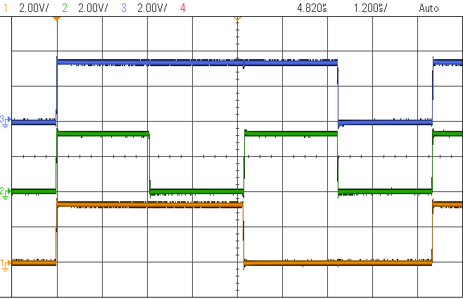
- For the AND example, two input
signals are used (the CLC in AND mode can have up to four inputs). The truth table
is shown below:
Table 1-19. Truth Table for 2-Input Logic AND Function A B O = A AND B 0 0 0 0 1 0 1 0 0 1 1 1 Figure 1-77 depicts the input and output signals of CLC2 as it performs the AND logic function:
- Signal 1 (Orange) is PWM3 output used as CLC2 Input A
- Signal 2 (Green) is PWM4 output used as CLC2 Input B
- Signal 4 (Red) is CLC2 output (logic AND between PWM3 and PWM4)
Figure 1-77. Oscillograms of CLC2 Performing Logic AND, Input Signals PWM3 and PWM4 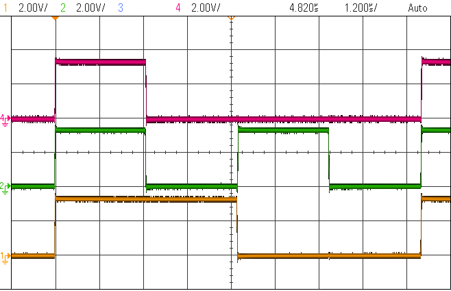
- For the XOR example, two input
signals are used. The truth table is shown below:
Table 1-20. Truth Table for 2-Input Logic XOR Function A B O = A XOR B 0 0 0 0 1 1 1 0 1 1 1 0 Figure 1-78 depicts the input and output signals of CLC3 as it performs the XOR logic function:
- Signal 1 (Orange) is PWM3 output used as CLC3 Input A
- Signal 2 (Green) is PWM4 output used as CLC3 Input B
- Signal 3 (Blue) is CLC3 output (logic XOR between PWM3 and PWM4)
Figure 1-78. Oscillograms of CLC3 Performing Logic XOR, Input Signals PWM3 and PWM4 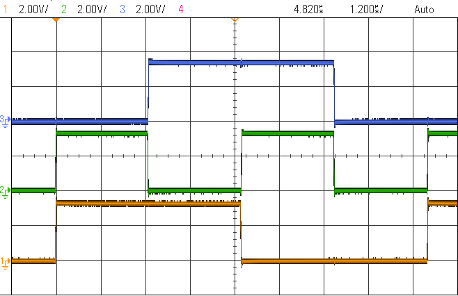
- System clock initialization
- Port initialization
- Timer initialization
- PWM initialization
- CLC initialization.
1.10.3.1 MCC Generated Code
To generate this project using MPLAB® Code Configurator (MCC), follow the next steps:
- Create a new MPLAB X IDE project for PIC18F47Q10.
- Open MCC from the toolbar. More information on how to install the MCC plug-in can be found here.
- Go to Project Resources →
System → System Module and do the following configuration:
- Oscillator Select: HFINTOSC
- HF Internal Clock: 64 MHz
- Clock Divider: 1
- In the Watchdog Timer Enable field in the WWDT tab, WDT Disabled has to be selected.
- In the Programming tab, Low-Voltage Programming Enable has to be checked.
- From the Device Resources window, add
TMR2, TMR4, PWM3, PWM4, CLC1, CLC2 and CLC3. Do the following configurations for
each peripheral:
- Timer2
Configuration:
- Enable Timer: checked
- Timer Clock
tab
- Clock Source: FOSC/4
- Prescaler: 1:1
- Postscaler: 1:1
- Timer Period: 10 us
- Enable Timer Interrupt: unchecked
- Timer4
Configuration:
- Enable Timer: checked
- Ext Reset Source: TMR2_postscaled
- Start/Reset Options: Resets at rising TMR4_rst
- Timer Clock
tab
- Clock Source: FOSC/4
- Prescaler: 1:1
- Postscaler: 1:1
- Timer Period: 5 us
- Enable Timer Interrupt: unchecked
- PWM3 Configuration:
- Enable PWM: checked
- Select a Timer: Timer2
- Duty Cycle: 50%
- PWM Polarity: active_hi
- PWM4 Configuration:
- Enable PWM: checked
- Select a Timer: Timer4
- Duty Cycle: 50%
- PWM Polarity: active_hi
- CLC1 Configuration:
- Enable CLC: checked
- Mode: AND-OR
- The AND-OR user configurable interpretation window is now available in the CLC1 window. Set the internal connections as shown below. By selecting PWM3 as both inputs for the AND, it becomes the first input of the OR. The same is true for PWM4 as second input of OR; this way CLC1 is used as a 2-input OR gate.
Figure 1-79 1-85 1-91. CLC1 Configuration Mode AND-OR, Used as 2-Input OR - CLC2 Configuration:
- Enable CLC: checked
- Mode: 4-input AND
- The 4-input AND user configurable interpretation window is now available in the CLC2 window. Set the internal connections as shown below. By selecting PWM3 as two of the inputs for the 4-input AND, and PWM4 as the other two, it becomes equivalent to a 2-input AND function from CLC2.
Figure 1-80 1-86. CLC2 Configuration Mode 4-Input AND, Used as 2-Input AND - CLC3 Configuration:
- Enable CLC: checked
- Mode: 4-input OR-XOR
- The OR-XOR user configurable interpretation window is now available in the CLC3 window. Set the internal connections as shown below. By selecting PWM3 as both inputs for the OR, it becomes the first input of the XO. The same is true for PWM4 as second input of XOR; this way CLC3 is used as a 2-input XOR gate.
Figure 1-81 1-87. CLC3 Configuration Mode OR-XOR, Used as 2-Input XOR
- Timer2
Configuration:
- In the Pin Manager: Grid View window,
select the I/O pins outputs to enable the internal signal access to the I/O as shown
in Figure 1-82 1-88 1-92.
Figure 1-82 1-88 1-92. Pin Mapping for the Example “Using Basic Logic Gates” - In the Project Resources window, click Generate.
For this example, no extra code was used aside from the one generated from MCC.

1.10.3.2 Bare Metal Code
The necessary code and functions to implement the presented example are analyzed in this section.
The first step will be to configure the microcontroller to disable the Watchdog Timer and to enable the Low-Voltage Programming (LVP).
#pragma config WDTE = OFF     /* WDT operating mode → WDT Disabled */
#pragma config LVP = ON       /* Low-voltage programming enabled, RE3 pin is MCLR */
As described in the example functionality, the following peripherals must be initialized: Timer2, Timer4, PWM3, PWM4, CLC1, CLC2, CLC3, the I/O PORT and PPS.
The internal oscillator has to be set to the desired value (in this case to 64 MHz), using the following function:
static void CLK_init(void)
{
    OSCCON1bits.NOSC = 6;   /* HFINTOSC oscillator */
    OSCFRQ = 0x08;          /* HFFRQ 64_MHz; */
}
To enable the output driver in the desired I/O pins (RA2, RA3, RB0, RC2 and RC3), the following function is used:
static void PORT_init(void)
{
    /* PORT RA2 and RA3 output driver enabled */
    TRISAbits.TRISA2 = 0;
    TRISAbits.TRISA3 = 0;
    /* PORT RB0 output driver enabled */
    TRISBbits.TRISB0 = 0;
    /* PORT RC2 and RC3 output driver enabled */
    TRISCbits.TRISC2 = 0;
    TRISCbits.TRISC3 = 0;
}
For Timer2 to use FOSC/4 as clock source and generate a pulse every 10 us (frequency = 100 kHz), the following function is used:
static void TMR2_init(void)
{
    T2CLKCONbits.CS = 1;  /* Timer2 clock source is FOSC/4 */
    T2PR = 0x9F;          /* Load period values */
    T2CON = 0x80;         /* Enable Timer2 */
}
Timer4 is configured to use FOSC/4 as clock source and generate a pulse every 5 us (frequency = 200 kHz). Timer4 is also set to start at the same time as Timer2. The following function is used:
static void TMR4_init(void)
{
    /* Timer4 clock source is FOSC/4 */
    T4CLKCONbits.CS = 1;
    /* Timer4 resets at rising TMR4_ers*/
    T4HLTbits.MODE = 4;
    /* Timer4 Reset source is TMR2_postscaled; */
    T4RSTbits.RSEL = 1;
    /* Load period values */
    T4PR = 0x4F;
    /* Enable Timer4 */
    T4CON = 0x80;
}
PWM3 uses Timer2 as pulse source and is configured to generate a pulse with 50% duty cycle. The following function is used:
static void PWM3_init(void)
 {
    PWM3CON = 0x80;   /* Enable PWM3*/
    /* Load duty cycle values */
    PWM3DCH = 0x4F;
    PWM3DCL = 0xC0;
    CCPTMRS = 0x10;   /* Select Timer2 as pulse source */
 }
PWM4 uses Timer4 as pulse source and it is configured to generate a pulse with 50% duty cycle. The following function is used:
static void PWM4_init(void)
 {
    PWM4CON = 0x80;           /* Enable PWM4*/
    /* Load duty cycle values */
    PWM4DCH = 0x27;
    PWM4DCL = 0xC0;
    CCPTMRSbits.P4TSEL = 2;   /*  Select Timer4 as pulse source */
 }
CLC1 is configured in the AND-OR mode and uses PWM3 and PWM4 as inputs with the instructions from the following function:
static void CLC1_init(void)
{
    CLC1POL = 0x00;    /* Clear the output polarity register */
    CLC1SEL0 = 0x1A;   /* Configure PWM3_OUT as input for first OR gate */
    CLC1SEL1 = 0x1A;   /* Configure PWM3_OUT as input for second OR gate */
    CLC1SEL2 = 0x1B;   /* Configure PWM4_OUT as input for third OR gate */
    CLC1SEL3 = 0x1B;   /* Configure PWM4_OUT as input for forth OR gate */
    /* All four inputs are not inverted*/
    CLC1GLS0 = 0x02;
    CLC1GLS1 = 0x08;
    CLC1GLS2 = 0x20;
    CLC1GLS3 = 0x80;
    CLC1CON = 0x80;    /* CLC1 enabled; Mode AND-OR*/
}
CLC2 is configured in the 4-input AND mode and uses PWM3 and PWM4 as inputs with the instructions from the following function:
static void CLC2_init(void)
{
    CLC2POL = 0x00;    /* Clear the output polarity register */
    CLC2SEL0 = 0x1A;   /* Configure PWM3_OUT as input for first OR gate */
    CLC2SEL1 = 0x1A;   /* Configure PWM3_OUT as input for second OR gate */
    CLC2SEL2 = 0x1B;   /* Configure PWM4_OUT as input for third OR gate */
    CLC2SEL3 = 0x1B;   /* Configure PWM4_OUT as input for forth OR gate */
    /* All four inputs are not inverted*/
    CLC2GLS0 = 0x02;
    CLC2GLS1 = 0x08;
    CLC2GLS2 = 0x20;
    CLC2GLS3 = 0x80;
    CLC2CONbits.EN = 1;     /* CLC2 enabled */
    CLC2CONbits.MODE = 2;   /* Mode 4-input AND */
}
CLC3 is configured in the OR-XOR mode and uses PWM3 and PWM4 as inputs with the instructions from the following function:
static void CLC3_init(void)
{
    CLC3POL = 0x00;    /* Clear the output polarity register */
    CLC3SEL0 = 0x1A;   /* Configure PWM3_OUT as input for first OR gate */
    CLC3SEL1 = 0x1A;   /* Configure PWM3_OUT as input for second OR gate */
    CLC3SEL2 = 0x1B;   /* Configure PWM4_OUT as input for third OR gate */
    CLC3SEL3 = 0x1B;   /* Configure PWM4_OUT as input for forth OR gate */
    /* All four inputs are not inverted*/
    CLC3GLS0 = 0x02;
    CLC3GLS1 = 0x08;
    CLC3GLS2 = 0x20;
    CLC3GLS3 = 0x80;
    CLC3CONbits.EN = 1;     /* CLC3 enabled */
    CLC3CONbits.MODE = 1;   /* Mode OR-XOR */
}
To measure the internal peripheral signals with the oscilloscope, the following link must be made:
| Internal CIP Signal | Microcontroller Pin |
|---|---|
| PWM3_OUT | RA2 |
| PWM4_OUT | RA3 |
| CLC1_OUT | RC2 |
| CLC2_OUT | RC3 |
| CLC3_OUT | RB0 |
This is done in the following function:
static void PPS_init(void)
{
    RA2PPS = 0x07;   /*Configure RA2 for PWM3 output*/
    RA3PPS = 0x08;   /*Configure RA3 for PWM4 output*/
    RB0PPS = 0x1A;   /*Configure RB0 for CLC3 output*/
    RC2PPS = 0x18;   /*Configure RC2 for CLC1 output*/
    RC3PPS = 0x19;   /*Configure RC3 for CLC2 output*/
}
1.10.4 Using CLCs to Create a Data Signal Modulator (DSM)
This example shows an initialization of the CLC in the J-K flip-flop with R mode and AND-OR mode for the implementation of a Data Signal Modulator (DSM) with timings controlled from the CCP peripheral. The truth table of the J-K flip-flop is shown below.
| CLK | J | K | O |
|---|---|---|---|
| 0 | 0 | 0 | Latch |
| 0 | 0 | 1 | 0 |
| 0 | 1 | 0 | 1 |
| 0 | 1 | 1 | Toggle |
| 1 | 0 | 0 | Latch |
| 1 | 0 | 1 | Latch |
| 1 | 1 | 0 | Latch |
| 1 | 1 | 1 | Latch |
CLC1 (J-K flip-flop 1) has Timer2 as clock source (which represents the first modulated frequency), while the carrier signal generated from the CCP is connected to the J gate of the J-K flip-flop. The K gate is left to logic 1. This allows the CLC to toggle when the J input is high and stay 0 when the J input is low.
CLC2 (J-K flip-flop 2) is connected in the same way with Timer4 as clock source and the negated CCP as input for the J gate. This CCP connection to the J gates ensures that one CLC is toggling while the other has the output set to 0 logic. CLC3 set in AND-OR mode is connecting CLC1 and CLC2 outputs to create a DSM.
The internal architecture is shown in Figure 1-83.

DSM setup configurations:
- Timer2 frequency = 1 MHz (1 us period)
- Timer4 frequency = 500 kHz (2 us period)
- Timer6 frequency = 62.5 kHz (16 us period)
- CCP1 has Timer6 as source and duty cycle = 50%
- CLC1 is set up as J-K flip-flop with R
- CLC2 is set up as J-K flip-flop with R
- CLC3 is set up as AND-OR: used as 2-input OR
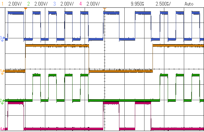
Figure 1-84 displays all the CLCs outputs and the CCP1 output side by side to show how this configuration implements the DSM function:
- Signal 1 (Orange) is CCP1 output
- Signal 2 (Green) is CLC1 output
- Signal 3 (Blue) is CLC3 output
- Signal 4 (Red) is CLC2 output
- System clock initialization
- Port initialization
- Timer initialization
- CCP initialization
- CLC initialization.
1.10.4.1 MCC Generated Code
To generate this project using MPLAB® Code Configurator (MCC), follow the next steps:
- Create a new MPLAB X IDE project for PIC18F47Q10.
- Open MCC from the toolbar. More information on how to install the MCC plug-in can be found here.
- Go to Project Resources →
System → System Module and do the following configuration:
- Oscillator Select: HFINTOSC
- HF Internal Clock: 64 MHz
- Clock Divider: 1
- In the Watchdog Timer Enable field in the WWDT tab, WDT Disabled has to be selected.
- In the Programming tab, Low-Voltage Programming Enable has to be checked.
- From the Device Resources window, add
TMR2, TMR4, TMR6, CCP1, CLC1, CLC2 and CLC3. Do the following configurations for
each peripheral:
- Timer2
Configuration:
- Enable Timer: checked
- Timer Clock
tab
- Clock Source: FOSC/4
- Prescaler: 1:1
- Postscaler: 1:1
- Timer Period: 1 us
- Enable Timer Interrupt: unchecked
- Timer4
Configuration:
- Enable Timer: checked
- Timer Clock
tab
- Clock Source: FOSC/4
- Prescaler: 1:1
- Postscaler: 1:1
- Timer Period: 2 us
- Enable Timer Interrupt: unchecked
- Timer6
Configuration:
- Enable Timer: checked
- Timer Clock
tab
- Clock Source: FOSC/4
- Prescaler: 1:1
- Postscaler: 1:1
- Timer Period: 16 us
- Enable Timer Interrupt: unchecked
- CCP1 Configuration:
- Enable CCP: checked
- CCP Mode: PWM
- Select Timer: Timer6
- Duty Cycle: 50%
- CCPR Alignment: right_aligned
- CLC1 Configuration:
- Enable CLC: checked
- Mode: J-K flip-flop with R
- The J-K flip-flop with R user configurable interpretation window is now available in the CLC1 window. Set the internal connections as shown below. By selecting TMR2 as clock source for the J-K, the CLC will generate a PWM signal with 500 kHz frequency and 50% duty cycle. Select CCP1 as the J input, allowing to have O = 0 when J is 0 and K is 1.
Figure 1-79 1-85 1-91. CLC1 Configuration Mode J-K Flip-Flop with R - CLC2 Configuration:
- Enable CLC: checked
- Mode: J-K flip-flop with R
- The J-K flip-flop with R user configurable interpretation window is now available in the CLC2 window. Set the internal connections as shown below. By selecting TMR as clock source for the J-K, the CLC will generate a PWM signal with 250 kHz frequency and 50% duty cycle. Select CCP1 as the J input, allowing to have O = 0 when J is 0 and K is 1.
Figure 1-80 1-86. CLC2 Configuration Mode J-K Flip-Flop with R - CLC3 Configuration:
- Enable CLC: checked
- Mode: AND-OR
- The AND-OR user configurable interpretation window is now available in the CLC3 window. Set the internal connections as shown below. By selecting CLC1 as both inputs for the AND, it becomes the first input of the OR. The same is true for CLC2 as second input of OR; this way CLC3 is used as a 2-input OR gate.
Figure 1-81 1-87. CLC3 Configuration Mode AND-OR, Used as 2-Input OR
- Timer2
Configuration:
- In the Pin Manager: Grid View window,
select the I/O pins outputs to enable the internal signal access to the I/O as
shown in Figure 1-82 1-88 1-92.
Figure 1-82 1-88 1-92. Pin Mapping for the Example “Using CLCs to Create a Data Signal Modulator” - In the Project Resources window, click Generate.
For this example, no extra code was used aside from the one generated from MCC.
1.10.4.2 Bare Metal Code
The necessary code and functions to implement the presented example are analyzed in this section.
The first step will be to configure the microcontroller to disable the Watchdog Timer and to enable the Low-Voltage Programming (LVP).
#pragma config WDTE = OFF     /* WDT operating mode → WDT Disabled */
#pragma config LVP = ON       /* Low-voltage programming enabled, RE3 pin is MCLR */
As described in the example functionality, the following peripherals must be initialized: Timer2, Timer4, Timer6, CCP1, CLC1, CLC2, CLC3, the I/O PORT and PPS.
The internal oscillator has to be set to the desired value (in this case to 64 MHz), using the following function:
static void CLK_init(void)
{
    OSCCON1bits.NOSC = 6;   /* HFINTOSC oscillator */
    OSCFRQ = 0x08;          /* HFFRQ 64_MHz; */
}
To enable the output driver in the desired I/O pins (RA2, RA3 and RB3), the following function is used:
static void PORT_init(void)
{
    /*PORT RA2 and RA3 output driver enabled*/
    TRISAbits.TRISA2 = 0;
    TRISAbits.TRISA3 = 0;
    /*PORT RB3 and RB0 output driver enabled*/
    TRISBbits.TRISB0 = 0;
    TRISBbits.TRISB3 = 0;
}
Timer2 is configured to use FOSC/4 as clock source and generate a pulse every 1 us (frequency = 1 MHz). Timer2 is also set to start at the same time as Timer4. The following function is used:
static void TMR2_init(void)
{
    T2CLKCONbits.CS = 1;  /* Timer2 clock source is FOSC/4 */
    T2HLTbits.MODE = 4;   /* Timer2 resets at rising TMR2_ers*/
    T2RSTbits.RSEL = 2;   /* Timer2 Reset source is TMR4_postscaled; */
    T2PR = 0x0F;          /* Load period values */
    T2CON = 0x80;         /* Enable Timer2 */
}
Timer4 is configured to use FOSC/4 as clock source and generate a pulse every 2 us (frequency = 200 kHz). The following function is used:
static void TMR4_init(void)
{
    T4CLKCONbits.CS = 1;   /* Timer4 clock source is FOSC/4 */
    T4PR = 0x1F;           /* Load period values */
    T4CON = 0x80;          /* Enable Timer4 */
}
Timer6 is configured to use FOSC/4 as clock source and generate a pulse every 16 us (frequency = 62.5 kHz). The following function is used:
static void TMR6_init(void)
{
    T6CLKCONbits.CS = 1;   /* Timer6 clock source is FOSC/4 */
    T6PR = 0xFF;           /* Load period values */
    T6CON = 0x80;          /* Enable Timer6 */
}
CCP1 works as a PWM with 50% duty cycle and Timer6 as pulse source. The following function is used:
static void CCP1_init(void)
 {
    CCP1CON = 0x8C;   /* Enable CCP1 in PWM mode*/
    /* Load duty cycle values */
    CCPR1H = 0x01;
    CCPR1L = 0xFF;
    CCPTMRS = 0x03;   /* Select Timer6 as pulse source*/
 }
CLC1 is configured in the J-K flip-flop with R mode and uses TMR2 and CCP1 as inputs. The following function is used:
static void CLC1_init(void)
{
    CLC1POL = 0x08;    /* Negated output for fourth OR gate*/
    CLC1SEL0 = 0x13;   /* Configure TMR2_OUT as input for first OR gate */
    CLC1SEL1 = 0x18;   /* Configure CCP1_OUT as input for second OR gate */
    CLC1SEL2 = 0x13;   /* Configure TMR2_OUT as input for third OR gate */
    CLC1SEL3 = 0x13;   /* Configure TMR2_OUT as input for forth OR gate */
    /* All four inputs are not inverted*/
    CLC1GLS0 = 0x02;
    CLC1GLS1 = 0x08;
    CLC1GLS2 = 0x00;
    CLC1GLS3 = 0x00;
    CLC1CONbits.EN = 1;     /* CLC1 enabled */
    CLC1CONbits.MODE = 6;   /* Mode J-K flip-flop with R */
}
CLC2 is configured in the J-K flip-flop with R mode and uses TMR4 and CCP1 as inputs. The following function is used:
static void CLC2_init(void)
{
    CLC2POL = 0x08;    /* Negated output for fourth OR gate*/
    CLC2SEL0 = 0x15;   /* Configure TMR4_OUT as input for first OR gate */
    CLC2SEL1 = 0x18;   /* Configure CCP1_OUT as input for second OR gate */
    CLC2SEL2 = 0x15;   /* Configure TMR4_OUT as input for third OR gate */
    CLC2SEL3 = 0x15;   /* Configure TMR4_OUT as input for forth OR gate */
    /* Inputs 1, 3 and 4 are not inverted; Input 2 inverted*/
    CLC2GLS0 = 0x02;
    CLC2GLS1 = 0x04;
    CLC2GLS2 = 0x00;
    CLC2GLS3 = 0x00;
    CLC2CONbits.EN = 1;     /* CLC2 enabled */
    CLC2CONbits.MODE = 6;   /* Mode J-K flip-flop with R */
}
CLC3 is configured in the AND-OR mode and uses CLC1 and CLC2 as inputs. The following function is used:
static void CLC3_init(void)
{
    CLC3POL = 0x00;    /* Clear the output polarity register */
    CLC3SEL0 = 0x21;   /* Configure CLC1_OUT as input for first OR gate */
    CLC3SEL1 = 0x21;   /* Configure CLC1_OUT as input for second OR gate */
    CLC3SEL2 = 0x22;   /* Configure CLC2_OUT as input for third OR gate */
    CLC3SEL3 = 0x22;   /* Configure CLC2_OUT as input for forth OR gate */
    /* All four inputs are not inverted*/
    CLC3GLS0 = 0x02;
    CLC3GLS1 = 0x08;
    CLC3GLS2 = 0x20;
    CLC3GLS3 = 0x80;
    CLC3CONbits.EN = 1;     /* CLC3 enabled */
    CLC3CONbits.MODE = 0;   /* Mode AND-OR */
}
To measure the internal peripheral signals with the oscilloscope, the following link must be made:
| Internal CIP Signal | Microcontroller Pin |
|---|---|
| CLC1_OUT | RA2 |
| CLC2_OUT | RA3 |
| CLC3_OUT | RB0 |
| CCP1_OUT | RB3 |
This is done in the following function:
static void PPS_init(void)
{
    RA2PPS = 0x18;   /*Configure RA2 for CLC1 output*/
    RA3PPS = 0x19;   /*Configure RA3 for CLC2 output*/
    RB0PPS = 0x1A;   /*Configure RB0 for CLC3 output*/
    RB3PPS = 0x05;   /*Configure RB3 for CCP1 output*/
}
1.10.5 Using the CLC to Create an LED Dimming Effect
This example shows an initialization of the CLC in the SR Latch mode for the implementation of an automatic fixed frequency with variable duty cycle PWM signal. The function is automatically called as it does not require code or core supervision to work. The hardware is set at start-up and can be reconfigured during run-time. The truth table of the SR Latch is shown below.
| S | R | O |
|---|---|---|
| 0 | 0 | 0 |
| 0 | 1 | 0 |
| 1 | 0 | 1 |
| 1 | 1 | 0 |
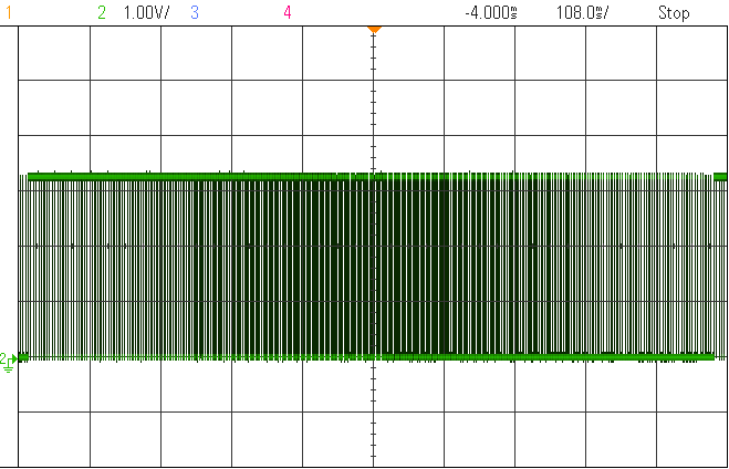
CLC1 (SR Latch) has Timer2 as S gate source (which creates the fixed frequency of the generated PWM), and connected at the R gate is Timer4 to generate the duty cycle of the PWM. Timer4 is set with a slightly higher frequency than Timer2. At each cycle, the duty cycle will get smaller with the difference between the two signals until it reaches zero and the process restarts. The difference between Timer2 and Timer4 represents the step of the duty cycle change, which in this case is 0.1 Hz (or 1 Least Significant Byte difference), and therefore creating 255 repetitive PWM signals.
When this PWM signal is connected to an LED, the created effect is that the LED is repetitively dimmed. If the signal is inversed, it creates the effect of repetitively increasing LED light (the kind of loading effect).
The internal architecture is shown in Figure 1-89.

Test setup configurations:
- Timer2 frequency = 24.41 Hz (4.096 ms period)
- Timer4 frequency = 24.51 Hz (4.08 ms period)
- CLC1 is set up as SR Latch
Figure 1-90 displays the CLC1 output implementing the fixed frequency with variable duty cycle function:
- Signal 2 (Green) is CLC1 output
- System clock initialization
- Port initialization
- Timer initialization
- CLC initialization.
1.10.5.1 MCC Generated Code
To generate this project using MPLAB® Code Configurator (MCC), follow the next steps:
- Create a new MPLAB X IDE project for PIC18F47Q10.
- Open MCC from the toolbar. More information on how to install the MCC plug-in can be found here.
- Go to Project Resources →
System → System Module and do the following configuration:
- Oscillator Select: HFINTOSC
- HF Internal Clock: 64 MHz
- Clock Divider: 1
- In the Watchdog Timer Enable field in the WWDT tab, WDT Disabled has to be selected.
- In the Programming tab, Low-Voltage Programming Enable has to be checked.
- From the Device Resources window, add
TMR2, TMR4 and CLC1. Do the following configurations for each peripheral:
- Timer2
Configuration:
- Enable Timer: checked
- Timer Clock
tab
- Clock Source: FOSC/4
- Prescaler: 1:128
- Postscaler: 1:2
- Timer Period: 4.096 ms
- Enable Timer Interrupt: unchecked
- Timer4
Configuration:
- Enable Timer: checked
- Timer Clock
tab
- Clock Source: FOSC/4
- Prescaler: 1:128
- Postscaler: 1:2
- Timer Period: 4.08 ms
- Enable Timer Interrupt: unchecked
- CLC1 Configuration:
- Enable CLC: checked
- Mode: SR Latch
- The SR Latch user configurable interpretation window is now available in the CLC1 window. Set the internal connections as shown below. By selecting TMR2 as clock source for the ‘S’ input and TMR4 as source for the ‘R’ input, the CLC will generate a PWM signal with 24.51 Hz frequency and variable duty cycle with steps equal to the difference between TMR2 and TMR4.
Figure 1-79 1-85 1-91. CLC1 Configuration Mode SR Latch
- Timer2
Configuration:
- In the Pin Manager: Grid View window,
select the I/O pins outputs to enable the internal signal access to the I/O as shown
in Figure 1-82 1-88 1-92.
Figure 1-82 1-88 1-92. Pin Mapping for the Example “Using the CLC to Create an LED Dimming Effect” - In the Project Resources window, click Generate.
For this example, no extra code was used aside from the one generated from MCC.
1.10.5.2 Bare Metal Code
The necessary code and functions to implement the presented example are analyzed in this section.
The first step will be to configure the microcontroller to disable the Watchdog Timer and to enable the Low-Voltage Programming (LVP).
#pragma config WDTE = OFF     /* WDT operating mode → WDT Disabled */
#pragma config LVP = ON       /* Low-voltage programming enabled, RE3 pin is MCLR */
As described in the example functionality, the following peripherals must be initialized: Timer2, Timer4, CLC1, the I/O PORT and PPS.
The internal oscillator has to be set to the desired value (in this case to 64 MHz), using the following function:
static void CLK_init(void)
{
    OSCCON1bits.NOSC = 6;   /* HFINTOSC oscillator */
    OSCFRQ = 0x08;          /* HFFRQ 64_MHz; */
}
To enable the output driver in the desired I/O pins (RA2), the following function is used:
static void PORT_init(void)
{
    TRISAbits.TRISA2 = 0;   /*PORT RA2 output driver enabled*/
}
For Timer2 to use FOSC/4 as clock source and generate a pulse every 4.096 ms (frequency = 24.41 Hz), the prescaller must also be added to 1:128 and postcaller to 1:2. The following function is used:
static void TMR2_init(void)
{
    T2CLKCONbits.CS = 1;   /* Timer2 clock source is FOSC/4 */
    T2PR = 0xFF;           /* Load period values */
    T2CONbits.CKPS = 7;    /* Set prescaller to 1:128 */
    T2CONbits.OUTPS = 1;   /* Set postcaller to 1:2 */
    T2CONbits.ON = 1;      /* Enable Timer2 */
}
For Timer4 to use FOSC/4 as clock source and generate a pulse every 4.08 ms (frequency = 24.51 Hz), the prescaller must also be added to 1:128 and postcaller to 1:2. The following function is used:
static void TMR4_init(void)
{
    T4CLKCONbits.CS = 1;   /* Timer4 clock source is FOSC/4 */
    T4PR = 0xFE;           /* Load period values */
    T4CONbits.CKPS = 7;    /* Set prescaller to 1:128 */
    T4CONbits.OUTPS = 1;   /* Set postcaller to 1:2 */
    T4CONbits.ON = 1;      /* Enable Timer4 */
}
CLC1 is configured in the SR Latch mode and uses TMR2 and TMR4 as inputs. The following function is used:
static void CLC1_init(void)
{
    CLC1POL = 0x00;    /* Clear the output polarity register */
    CLC1SEL0 = 0x13;   /* Configure TMR2_OUT as input for first OR gate */
    CLC1SEL1 = 0x13;   /* Configure TMR2_OUT as input for second OR gate */
    CLC1SEL2 = 0x15;   /* Configure TMR4_OUT as input for third OR gate */
    CLC1SEL3 = 0x15;   /* Configure TMR4_OUT as input for fourth OR gate */
    /* All four inputs are not inverted*/
    CLC1GLS0 = 0x02;
    CLC1GLS1 = 0x08;
    CLC1GLS2 = 0x20;
    CLC1GLS3 = 0x80;
    CLC1CONbits.EN = 1;     /* CLC1 enabled; */
    CLC1CONbits.MODE = 3;   /* Mode SR latch */
}
To measure the internal peripheral signals with the oscilloscope, the following link must be made:
| Internal CIP Signal | Microcontroller Pin |
|---|---|
| CLC1_OUT | RA2 |
This is done in the following function:
static void PPS_init(void)
{
    RA2PPS = 0x18;    /*Configure RA2 for CLC1 output*/
}