
1.2 PIC1000 Getting Started Writing C-code for PIC16 and PIC18
1.2.1 Introduction
| Authors: Cristian Săbiuţă, Cristina Ionescu, Microchip Technology Inc. |
This technical brief provides the steps recommended to successfully program a PIC16 or PIC18 microcontroller and defines coding guidelines to help write more readable and reusable code.
High-level programming languages are a necessity due to imposed short development time and high-quality requirements. These languages make it easier to maintain and reuse code due to better portability and readability than the low-level instructions specific for each microcontroller architecture.
Programming language alone does not ensure high readability and reusability, but good coding style does. Therefore, the PIC® peripherals, header files and drivers are designed according to this presumption.
Since the most widely used high-level programming language for PIC microcontrollers is C, this document will focus on C programming. To ensure compatibility with most PIC C compilers, the code examples in this document are written using ANSI C coding standard.
1.2.2 Data Sheet Module Structure and Naming Conventions
The first step in writing C-code for a microcontroller is knowing and understanding the type of information found in the data sheet of the device used for programming. The data sheet contains information about the features, memories, core and peripheral modules of the microcontroller. Also included in the data sheet are the functional descriptions and base addresses of the peripheral modules, the names and addresses of the registers and other functional and electrical characteristics.
1.2.2.1 How to Find the Data Sheet
The data sheet for the PIC16F and PIC18F microcontroller families can be found at:
- Microchip Data Sheet page
1.2.2.2 Pin Description
The pin description can be found in any device data sheet. The pinout is contained in the data sheet’s Pin Diagrams chapter, which covers various devices depending on the pin or package specifications. The TQFP pinout of the PIC18-Q10 44-pin devices is presented in Figure 1-1.

The Pin Allocation Tables chapter from the PIC18F27/47Q10 data sheet contains information about the pre-established pin functions. These functionalities that can be configured for each I/O pin are usually input or output of peripheral modules instances. This information varies depending on the device number of pins. If an evaluation board is used, such as the PIC18F47Q10 Curiosity Nano Development Platform, the routing of the pins on the specific board must be known. The information is available at PIC18F47Q10 Curiosity Nano page.
1.2.2.3 Modules Description
A PIC microcontroller is comprised of several building blocks: a PIC CPU core, SRAM, Flash, EEPROM, and various peripheral modules called module types. Throughout this document, all peripheral modules will be referred to as modules.
Newer PIC families of microcontrollers can have one or more instances of a given module type. All instances of a module have the same features and functions. There can be some modules that are a subset of other module types and inherit some of their features. The inherited features are fully compatible with the respective module type. For example, the subset module for a timer can have fewer compare and capture channels than a full timer module.

A module type can be the Enhanced Universal Synchronous Asynchronous Receiver Transmitter (EUSART), while the module instance is, for example, ‘EUSART1’, where the ‘1’ suffix indicates that the instance is ‘EUSART number 1’. For simplicity, a module instance will be referred to as a module throughout this document, unless there is a need to differentiate.
Each module has several registers that contain control or status bits. All modules of a given type contain the same set or subset of registers. All of these registers contain the same set or subset of control and status bits.
All of the registers corresponding to a module have a fixed address in the I/O memory map. This way, each register will be available at an absolute address specified by the data sheet.
Every module has a dedicated chapter that presents the features of the module, a functional description of the module and the specific signals and guidelines on how to configure a certain mode of operation with all the terminology explained. At the end of a module chapter, the Register Definitions subchapter contains the scope of every register, the reset values of the registers, and whether or not it is readable or writable. It also provides the position of every configurable/accessible bit of a register.
All the registers, their addresses, and the bit names and positions are described in the Register Summary section for each module. The register summary for the ADC module is presented in Figure 1-3.
For examples on how to access the ADGO bit from the ADCON0 register, refer to section 2.1.1. Register Unions
1.2.2.4 Naming Conventions
This section describes the register and bit naming conventions that can be found in the device data sheet.
1.2.2.4.1 Register Naming Conventions
Registers are divided into Control (CON), Status (STA) and Data registers with their naming reflecting this. A general purpose control register of a module has the control identifier named CON. If multiple general purpose control registers exist in a module, they have a suffix number identifier. In this case, the control registers will be named CON0, CON1, CON2 and so on. For example, see ADCON0, ADCON1, ADCON2 and ADCON3 registers in Figure 1-3.
When there are multiple instances of the same peripheral in a device, the name of the peripheral control registers will be depicted as the concatenation of the peripheral identifier, the peripheral instance number and the control identifier. Therefore, all the register names of PIC microcontrollers are unique. For example, in Figure 1-4, observe the RC2STA (Receive Status and Control Register) for EUSART peripheral instance 2.
For registers that have a specific function, their name reflects this functionality. For example, BAUD2CON is the Baud Rate Control Register for the second instance of the EUSART peripheral.
Since the PIC data bus width is 8 bits, larger registers are implemented using several 8-bit registers. For a 16-bit register, the high and low bytes are accessed by appending ‘H’ and ‘L’ respectively to the register name. For example, the ADC Result Register is named ADRES and the two bytes are ADRESL and ADRESH.
After the Register Summary section in the device data sheet, each register has a Register Definition section, which fully describes the functionality of each bit and bit field in the register. The Register Definitions section shows one instance of all the register names with an ‘x’ in place of the peripheral instance number. An example is presented in Figure 1-5.
1.2.2.4.2 Bit Naming Conventions
Since the prefix for the peripheral module type is unique, each bit name described in the data sheet is unique.
The device header file offers some register bits a Short Bit Name alternative consisting of only the bit function abbreviation. Since this is defined in the context of a bit union for a specific register, the bit access remains unique. For further details on how to access a bit using the short or long naming convention, refer to 2.1.1 Register Unions.
1.2.2.4.3 Register and Bit Naming Exceptions
Status, Interrupt, and Mirror Bits
Status, Interrupt Enable, Interrupt Flag, and Mirror bits are contained in registers that span across more than one peripheral. In these cases, the bit name shown is unique, and there is no prefix or short name variant.
Legacy Peripherals
There are some peripherals that do not strictly adhere to this naming convention. These are the peripherals that have existed for many years and are present in almost every device. These exceptions were necessary to limit the adverse impact of the new conventions on legacy code. Peripherals that do adhere to the new convention will include a table in the register section indicating the long name prefix for each peripheral instance. Peripherals that fall into the exception category will not have this table. These peripherals include, but are not limited to the following:
- Enhanced Universal Asynchronous Receiver Transceiver (EUSART)
- Master Synchronous Serial Port (MSSP)
1.2.2.5 PIC® Configuration Bits
Configuration bits are a collection of specialized bits that can only be modified at program time. Configuration bits are read during reset and enable or disable hardware features in the microcontroller. The features controlled by the configuration bits include, but are not limited to, the clock source, the Watchdog Timer (WDT), the Brown-Out Detector (BOD), and the Memory Read protection. Configuration bits are not executable code. Essentially, they are fuses located in the program memory space.
Each PIC microcontroller has its own set of configuration bits. The Device Configuration section of the individual data sheets contains the definition for each of the bits. See below an example from the PIC16F18446 data sheet.
For further details on how to set the Configuration Bits consult the 3.4 Setting Configuration Bits section.
1.2.3 Modules Representation in Header Files
A dedicated header file is available for each PIC device. If the target device is specified in the project settings, the MPLAB® XC8 Compiler will automatically include the correct header file if the device file is included as shown below:
#include <xc.h>All of the required register macro definitions can be found in the header file along with bit masks, bit field masks, bit positions and union definitions for the registers. The macros and struct definitions which are already defined in the device specific header file can be used instead of using a register's address.
This is useful for devices that contain the same module and where the header file definitions for that module are identical.
1.2.3.1 Registers Representation in Header Files
The I/O memory map is laid out so that all registers for a given peripheral module are placed in one continuous memory block. Registers belonging to different modules are not mixed up, where the registers macros are defined as below:
#define LATA LATA
extern volatile unsigned char           LATA                __at(0xF82);
#define LATB LATB
extern volatile unsigned char           LATB                __at(0xF83);
#define LATC LATC
extern volatile unsigned char           LATC                __at(0xF84);
1.2.3.1.1 Register Unions
Each register has a union declared in the header file for the individual bits in that register. This allows access to an individual bit/bit field from the register using the union declaration.
typedef union {
    struct {
        unsigned ADGO                   :1;
        unsigned                        :1;
        unsigned ADFM                   :1;
        unsigned                        :1;
        unsigned ADCS                   :1;
        unsigned                        :1;
        unsigned ADCONT                 :1;
        unsigned ADON                   :1;
    };
    struct {
        unsigned GO                     :1;
        unsigned                        :1;
        unsigned ADFM0                  :1;
    };
} ADCON0bits_t;
extern volatile ADCON0bits_t ADCON0bits __at(0xF5B);
The union declaration of the ADCON0 register is shown in the code listing above. This register can be accessed as a whole using the macro declaration or as an individual bit/bit field from the register using the union declaration. Here is an example:
ADCON0 = 0x01;       /* using macro declaration */
ADCON0bits.GO = 1;   /* using bit unions with short bit name convention */
ADCON0bits.ADGO = 1; /* using bit unions with long bit name convention */

For further details on unions, consult Microchip Developer - Unions.
1.2.3.1.2 Multibyte Registers
Some registers are used in conjunction with other registers to represent 16-bit values. These registers can be accessed as a whole using the register macro or by accessing the low/high bytes using the ‘L’/’H’ suffixes attached to the register macro. For example, the 16-bit ADC Result register has the following declaration in the header file:
#define ADRES ADRES
extern volatile unsigned short          ADRES               __at(0xF5E);
#define ADRESL ADRESL
extern volatile unsigned char           ADRESL              __at(0xF5E);
#define ADRESH ADRESH
extern volatile unsigned char           ADRESH              __at(0xF5F);
1.2.3.2 Bit Masks and Bit Field Masks
Register bits can be manipulated using predefined masks, or bit positions. The predefined bit masks from the header file are either related to individual bits, called a bit mask, or related to a bit field, called a bit field mask.
A bit mask is used both when setting and clearing individual bits. A bit field mask is mainly used when clearing multiple bits in a bit field.
For the ADCON2 register, the bit fields, bit names, bit positions, and bit masks of this register, see the table below.
| Bit Field | - | ADCRS | - | ADMD | ||||
|---|---|---|---|---|---|---|---|---|
| Bit Name | ADPSIS | ADCRS2 | ADCRS1 | ADCRS0 | ADACLR | ADMD2 | ADMD1 | ADMD0 |
| Bit Position | 7 | 6 | 5 | 4 | 3 | 2 | 1 | 0 |
| Bit Mask | 0x80 | 0x40 | 0x20 | 0x10 | 0x08 | 0x04 | 0x02 | 0x01 |
1.2.3.2.1 Bit Masks
The bit masks are predefined in the device header file. For example, the bit mask for the ADPSIS bit is defined as below.
#define _ADCON2_ADPSIS_MASK 0x80The naming convention adopted for the predefined bit masks in the header file is presented in Figure 2-2 with an example for the ADPSIS bit in the ADCON2 register.

1.2.3.2.2 Bit Field Masks
Many functions are controlled by a bit field. For example, ADCRS[2:0] and ADMD[2:0] in the ADCON2 register are grouped bits. The value of the bits in a field selects a specific configuration.
When changing bits in a bit field, it is not enough to set the bits for the desired configuration. It is also required to clear the bits from the old configuration before assigning a new value. To facilitate this, a bit field mask is defined.
The field masks are predefined in the device header file. For example, the field mask for the ADMD bit field is defined below.
#define _ADCON2_ADMD_MASK 0x7The naming convention adopted for the predefined bit field masks in the header file is presented in the Figure 2-3 with an example for the ADMD bit field in the ADCON2 register.

The bits from a bit field can be accessed as individual bits. To differentiate between these bits, a suffix (index of each bit in the bit field) is appended to the bit field name. The masks for the bits in a bit field are defined below.
#define _ADCON2_ADMD0_MASK                                  0x1
#define _ADCON2_ADMD1_MASK                                  0x2
#define _ADCON2_ADMD2_MASK                                  0x4
For further details on bit fields, consult Microchip Developer - Bit Fields.
1.2.3.3 Bit Positions
It is possible to use bit positions as an alternative to set or clear bits. A bit position within a register is defined using the same naming convention used at the bit masks, with the ‘_POSITION’ suffix instead of ‘_MASK’. There is also another definition for the bit positions in the header file. This bit position definition has the same functionality, but the suffix is ‘_POSN’. This is implemented for compatibility reasons.

The bit position definition for the ADPSIS bit from the header file is shown below.
#define _ADCON2_ADPSIS_POSN                                 0x7
#define _ADCON2_ADPSIS_POSITION                             0x7
The bit positions are included for compatibility reasons. They are also needed when programming in assembly for instructions that use a bit number.
1.2.4 Writing Bare Metal C-Code for PIC
The following section focuses on how to write C-code for the PIC16 and PIC18 microcontroller families. The examples describe how to make the code highly readable and portable between different PIC16 and PIC18 devices. The examples can also be used as a guideline on how to write code that is easy to verify and maintain.
PIC registers are located in dedicated and continuous blocks in the memory space and can be seen as encapsulated units. This reflects on the way that the registers are accessed when coding in C. Registers are encapsulated using C unions, in which all the bits and bit fields are encapsulated using C structs. A register can be accessed as a whole using the macro declaration of the register or it can be accessed using the union declaration of the register. A bit field can be accessed similarly to the register.
This document introduces a naming convention and register access method that is compliant with the PIC header files. This provides readability and portability to the codes written in C-code.
1.2.4.1 Set, Clear and Read Register Bits
Setting and clearing register bits are fundamental operations used in embedded programming. Applications are based on this technique.
The Read-Modify-Write (RMW) operations are a class of atomic operations that both read a memory location and write a new value to it simultaneously, either with a completely new value or some part of the previous value.
Since it has a wide applicability, reading the value of a bit is mainly used
in conditional expressions (e.g. if statement) and as a condition in
loop expressions (e.g. while statement). A common use case of this
technique is polling on an interrupt flag (reading the value of the bit and executing a
set of instructions if the bit is set/clear).
1.2.4.1.1 Set, Clear and Read Register Bits using Bit Unions
The recommended coding style to set or clear a specific bit in a register is to use the union declaration of the register from the header file.
The example below shows how to set and clear the Enable bit from the ADCON0 register using the recommended coding style.
ADCON0bits.ADON = 1; /* the ADC Enable bit is set */
ADCON0bits.ADON = 0; /* the ADC Enable bit is cleared */
/* wait while the ADGO bit is set */
while(ADCON0bits.ADGO)
{
    /* wait */
}The code listing below shows how to read the value of a PORT pin using bit unions and execute a set of instructions if that pin is low.
/* if pin 0 of the PORTA is clear execute a set of instructions */
if(!PORTAbits.RA0)
{
    /* set of instructions */
}
1.2.4.1.2 Set, Clear and Read Register Bits using Bit Masks
There are alternative ways to set and clear register bits by using bit masks or bit positions.
In order to set a bit from a register using bit masks, the binary OR operator will be applied between the register and the bit mask. Using the binary OR operator will ensure that the other bit settings made inside the register will remain the same and unaffected by this operation.
ADCON0 |= _ADCON0_ADON_MASK; /* the ADC Enable bit is set */In order to clear a bit from a register using bit masks, the binary AND operator will be applied between the register and the negated value of the bit mask. This operation also keeps the other bit settings unchanged.
ADCON0 &= ~_ADCON0_ADON_MASK; /* the ADC Enable bit is cleared */The bit mask for the ADC Enable bit (ADON) has the following declaration in the header file.
#define _ADCON0_ADON_MASK 0x80The code listing below shows how to read the value of a PORT pin using bit masks and execute a set of instructions if that pin is low.
if(PORTA & _PORTA_RA0_MASK)
{
    /* set of instructions */
}
1.2.4.1.3 Set, Clear and Read Register Bits using Bit Positions
In order to set a bit from a register using bit positions, the binary OR operator will be
applied between the register and the value resulting from shifting ‘1’
with the value of the bit position. To clear a bit using bit positions the binary AND
operator is used with the negated value of the shifting result.
ADCON0 |= (1 << _ADCON0_ADON_POSITION);  /* the ADC Enable bit is set */
ADCON0 &= ~(1 << _ADCON0_ADON_POSITION); /* the ADC Enable bit is cleared */
#define _ADCON0_ADON_POSITION 0x7The code listing below shows how to read the value of a PORT pin using bit positions and execute a set of instructions if that pin is low.
if(PORTA & (1<< _PORTA_RA0_POSITION))
{
    /* set of instructions */
}
1.2.4.2 Register Initialization
In order to initialize a register, the user must find the desired configuration of the register to achieve the expected functionality by consulting the device data sheet and setting or clearing register bits, so that the value in the register matches the desired configuration.
Register initialization is most often performed as part of device initialization after
reset, when the register is in a known state of '0'. This is a special
use-case, since:
- The register value may be
0x00 - Various bits and bit fields need to be configured at once
Read-modify-write operations are not needed, when working with bit masks or bit
positions, if the reset value of the register is 0x00 and the register
configures in a single line.
0’, but there are exceptions. For example, the Peripheral
Interrupt Priority Register 3 has several bits with the reset value
‘1’. In this case, the user has to explicitly set the desired
configuration without relying on the fact that usually bits reset values are
0. The reset value for all bits and bit fields in a register are
shown in the figure below.The following example will apply the various methods of configuring a register (T0CON0 – Timer 0 Control Register 0), shown in the figure below.
0’ after reset. - Enable the timer - T0EN =
1 - Select 8-bit mode - T016BIT =
0(default) - Select a 1:10 postscaler -
T0OUTPS =
1001(changed in 3.3 Change Register Bit Field Configuration to0111)
The resulting value can be directly written to the register:
T0CON0 = 0b1000 1001;    /* binary */
T0CON0 = 0x89;           /* hexadecimal */
T0CON0 = 137;            /* decimal */
However, to improve the readability (and potentially the portability) of the code, it is recommended to use the device defines, which are shown in the upcoming sections.
1.2.4.2.1 Register Initialization using Bit Unions
Register initialization using bit and bit field unions will always need to be done in several lines of code, if configuring more than one bit or bit field.
The example below shows the recommended way of initializing a register, by using the union declaration of the register from the header file.
T0CON0bits.T0EN = 1;      /* Enable TMR0 */
T0CON0bits.T016BIT = 0;   /* Select 8-bit operation mode */
T0CON0bits.T0OUTPS = 0x9; /* Select 1:10 postscaler */
1.2.4.2.2 Register Initialization using Bit Masks
Read-modify-write operations are not needed, when working with bit masks or bit
positions, if the reset value of the register is 0x00 and the register
configures in a single line.
The example below shows how to achieve the same configuration using bit masks.
T0CON0 = _T0CON0_T0EN_MASK      /* Enable TMR0 */
       | _T0CON0_T0OUTPS0_MASK  /* Select 1:10 postscaler */
       | _T0CON0_T0OUTPS3_MASK; /* 8-bit operation mode selected by default */
/* incorrect initialization of the T0CON0 register */
T0CON0 = _T0CON0_T0EN_MASK;
T0CON0 = _T0CON0_T0OUTPS0_MASK;
T0CON0 = _T0CON0_T0OUTPS3_MASK;
In this example, no mask is used to explicitly configure the timer in the 8-bit mode. This is
possible because the reset value of the T016BIT is '0' which corresponds
to the 8-bit mode. To emphasize the configuration of this bit as 0, the
user could explicitly select the desired 8-bit mode by using a read-modify-write
operation. However, this would need to be a separate line of code and would leave the
register unchanged:
T0CON0 = _T0CON0_T0EN_MASK       /* Enable TMR0 */
       | _T0CON0_T0OUTPS0_MASK   /* Select 1:10 postscaler */
       | _T0CON0_T0OUTPS3_MASK;
T0CON0 &= ~_T0CON0_T016BIT_MASK; /* Select 8-bit operation mode explicitly */
1.2.4.2.3 Register Initialization using Bit Positions
Read-modify-write operations are not needed, when working with bit masks or bit
positions, if the reset value of the register is '0' and the register
configures in a single line.
The code listing below shows how to initialize a register using bit positions.
T0CON0 = (1 << _T0CON0_T0EN_POSITION)      /* Enable TMR0 */
       | (0 << _T0CON0_T016BIT_POSITION)   /* A placeholder to select 16-bit mode*/
       | (1 << _T0CON0_T0OUTPS0_POSITION)
       | (1 << _T0CON0_T0OUTPS3_POSITION); /* Select 1:10 postscaler */
1.2.4.2.4 Change Register Bit Field Configurations
This section covers considerations when updating a register bit field using various header file defines. The following bit field will be used as an example, where an update is needed, compared to the initialization configuration covered in 3.2. Register Initialization section.
- Select a 1:10 postscaler - T0OUTPS:
1001(previous setting) - Select a 1:8 postscaler - T0OUTPS:
0111(new setting)
Change Register Bit Field Configurations using Bit Unions
The union declaration of the registers offers access to register bits and bit fields without affecting the rest of the register.
/* using a hex value */
T0CON0bits.T0OUTPS = 0x7;     /* Select 1:10 postscaler */
/* using a binary value */
T0CON0bits.T0OUTPS = 0b0111;  /* Select 1:10 postscaler */
This is the recommended way of updating bit field register configurations, which is simpler than the alternative options.
Change Register Bit Field Configurations using Bit Masks
When updating only a bit field in a register, a read-modify-write must be used, to keep the other settings unaffected. Therefore, in order to change the configuration of a register bit field, it is recommended to first clear the bit field and then set a new configuration. However, in order to avoid putting the register in an unintended state between the clear and setting the new configuration, this should be done in a single line of code. For simplicity, the steps are first covered individually.
The bit field masks can be used to clear a bit field before assigning a new configuration. In the example, the T0OUTPS bit field mask is used to clear bit field.
/* The T0OUTPS bit field is cleared (Selecting a postscaler of 1:1 (T0OUTPS = 0)) */
T0CON0 &= ~_T0CON0_T0OUTPS_MASK;
/* Selecting new configuration (0b0111) of the T0OUTPS bit field */
T0CON0 |= _T0CON0_T0OUTPS2_MASK | _T0CON0_T0OUTPS1_MASK | _T0CON0_T0OUTPS0_MASK;
The bit field mask for the TMR0 Output Postscaler Select (T0OUTPS) has the following declaration in the header file.
#define _T0CON0_T0OUTPS_MASK 0xF
These steps must be implemented in a single line to avoid putting the microcontroller in an unintended state.
T0CON0 = (T0CON0 & ~_T0CON0_T0OUTPS_MASK) | _T0CON0_T0OUTPS2_MASK
                                          | _T0CON0_T0OUTPS1_MASK
                                          | _T0CON0_T0OUTPS0_MASK;
0).Change Register Bit Field Configurations using Bit Positions
The example below shows how to update a register bit field using bit positions to set the new configuration. Similar to the process of updating a register configuration using bit masks, the current configuration must be cleared and the new configuration set, in a single line of code.
/* Changing a bit field configuration with bit positions */
T0CON0 = (T0CON0 & ~_T0CON0_T0OUTPS_MASK) | (0 << _T0CON0_T0OUTPS3_POSITION)
                                          | (1 << _T0CON0_T0OUTPS2_POSITION)
                                          | (1 << _T0CON0_T0OUTPS1_POSITION)
                                          | (1 << _T0CON0_T0OUTPS0_POSITION);
T0CON0 = (T0CON0 & ~_T0CON0_T0OUTPS_MASK) | (1 << _T0CON0_T0OUTPS2_POSITION)
                                          | (1 << _T0CON0_T0OUTPS1_POSITION)
                                          | (1 << _T0CON0_T0OUTPS0_POSITION);
1.2.4.3 Change Register Bit Field Configurations
This section covers considerations when updating a register bit field using various header file defines. The following bit field will be used as an example, where an update is needed, compared to the initialization configuration covered in 3.2. Register Initialization section.
- Select a 1:10 postscaler - T0OUTPS:
1001(previous setting) - Select a 1:8 postscaler - T0OUTPS:
0111(new setting)
1.2.4.3.1 Change Register Bit Field Configurations using Bit Unions
The union declaration of the registers offers access to register bits and bit fields without affecting the rest of the register.
/* using a hex value */
T0CON0bits.T0OUTPS = 0x7;     /* Select 1:10 postscaler */
/* using a binary value */
T0CON0bits.T0OUTPS = 0b0111;  /* Select 1:10 postscaler */
This is the recommended way of updating bit field register configurations, which is simpler than the alternative options.
1.2.4.3.2 Change Register Bit Field Configurations using Bit Masks
When updating only a bit field in a register, a read-modify-write must be used, to keep the other settings unaffected. Therefore, in order to change the configuration of a register bit field, it is recommended to first clear the bit field and then set a new configuration. However, in order to avoid putting the register in an unintended state between the clear and setting the new configuration, this should be done in a single line of code. For simplicity, the steps are first covered individually.
The bit field masks can be used to clear a bit field before assigning a new configuration. In the example, the T0OUTPS bit field mask is used to clear bit field.
/* The T0OUTPS bit field is cleared (Selecting a postscaler of 1:1 (T0OUTPS = 0)) */
T0CON0 &= ~_T0CON0_T0OUTPS_MASK;
/* Selecting new configuration (0b0111) of the T0OUTPS bit field */
T0CON0 |= _T0CON0_T0OUTPS2_MASK | _T0CON0_T0OUTPS1_MASK | _T0CON0_T0OUTPS0_MASK;
The bit field mask for the TMR0 Output Postscaler Select (T0OUTPS) has the following declaration in the header file.
#define _T0CON0_T0OUTPS_MASK 0xF
These steps must be implemented in a single line to avoid putting the microcontroller in an unintended state.
T0CON0 = (T0CON0 & ~_T0CON0_T0OUTPS_MASK) | _T0CON0_T0OUTPS2_MASK
                                          | _T0CON0_T0OUTPS1_MASK
                                          | _T0CON0_T0OUTPS0_MASK;
0).1.2.4.3.3 Change Register Bit Field Configurations using Bit Positions
The example below shows how to update a register bit field using bit positions to set the new configuration. Similar to the process of updating a register configuration using bit masks, the current configuration must be cleared and the new configuration set, in a single line of code.
/* Changing a bit field configuration with bit positions */
T0CON0 = (T0CON0 & ~_T0CON0_T0OUTPS_MASK) | (0 << _T0CON0_T0OUTPS3_POSITION)
                                          | (1 << _T0CON0_T0OUTPS2_POSITION)
                                          | (1 << _T0CON0_T0OUTPS1_POSITION)
                                          | (1 << _T0CON0_T0OUTPS0_POSITION);
T0CON0 = (T0CON0 & ~_T0CON0_T0OUTPS_MASK) | (1 << _T0CON0_T0OUTPS2_POSITION)
                                          | (1 << _T0CON0_T0OUTPS1_POSITION)
                                          | (1 << _T0CON0_T0OUTPS0_POSITION);
1.2.4.4 Setting Configuration Bits
It is unlikely that a new C program will run properly on the device, even though the program is valid. All Microchip 8-bit devices must be configured to ensure correct operation. Some configuration settings affect fundamental operation of the device, such as those for the instruction clock.
- Not setting the Configuration Bits can prevent even blinking an LED. Even if the TRIS register is set up and a value is written to the port, there are several things that can prevent such seemingly simple program from working.
- Ensure that the device's Configuration registers are set up correctly. Also, the user must make sure that every bit in these registers is explicitly specified, not leaving them in their default state. All the configuration features are described in the device data sheet. If the Configuration Bits that specify the oscillator source are wrong, for example, the device clock cannot be running.
- For more information, refer to the MPLAB XC8 C Compiler User’s Guide.
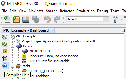
1.2.4.4.1 Accessing XC8 Configuration Bits Examples
To configure the device using MPLAB X Integrated Development Environment (IDE), the user must use configuration pragmas. More information about the compiler and the configuration bits of the desired device can be found by accessing the Compiler Help, the blue question mark from the MPLAB X IDE project dashboard, as presented in the figure below.
Example configurations can be found for specific devices under the Configuration Settings Reference section. An example for the PIC16F18446 is shown below.

1.2.4.4.2 MPLAB® X IDE Support for Setting Configuration Bits
The easiest way to complete the pragmas that are required to configure the device is to use the Configuration Bits Window, a feature of MPLAB X IDE.
Follow these steps to get the information to complete the pragmas:
- Open the Configuration Bits Window (Window > Target Memory Views > Configuration Bits or Production > Set Configuration Bits).
- Review every setting in the Configuration Bits Window.
- Generate the pragma derivatives that implement the chosen settings by clicking the Generate Source Code to Output button.
- Copy the generated code from this window to a source file.
- Consult the MPLAB XC8 Getting Started Guide, Specifying Device Configuration Bits section.
- Microchip Developer Help: View and Set Configuration Bits.
- Consult the video MPLAB X IDE Advanced Debugging - Event Breakpoints.
1.2.5 Application Example Showing Alternative Ways of Writing Code
The example below demonstrates how to configure the microcontroller to turn on an LED when a user button is pressed. To achieve this, the user needs to identify the pins of the microcontroller routed to the user LED and to the user button. This example is developed for the PIC18F47Q10 Curiosity Nano development board. The user LED is routed to the pin 0 of the PORTE. The user button is routed to the pin 2 of the PORTE.
1.2.5.1 Turn ON an LED on a Button Press using Bit Unions
The code below provides the described functionality following the recommended coding style by using the union declaration of the registers from the data sheet.
#include <xc.h>

void main(void)
{
    /* setting pin RE0 as output (LED) */
    TRISEbits.TRISE0 = 0;
    /* setting pin RE2 as input (button) */
    TRISEbits.TRISE2 = 1;
    /* enable digital input buffer for pin RE2 (button) */
    ANSELEbits.ANSELE2 = 0;
    /* enable internal pull-up for pin RE2 (button) */
    WPUEbits.WPUE2 = 1;

    /* main program loop */
    while(1)
    {
        /* if button is pressed (pin RE2 high) */
        if(PORTEbits.RE2)
        {
            /* turn on the LED (pin RE0 high) */
            LATEbits.LATE0 = 1;
        }
        else
        {
            /* turn off the LED (pin RE0 low) */
            LATEbits.LATE0 = 0;
        }
    }
}
1.2.5.2 Turn ON an LED on a Button Press using Bit Masks
The code below provides the same functionality using bit masks.
#include <xc.h>

void main(void)
{
    /* setting pin RE0 as output (LED) */
    TRISE &= ~_TRISE_TRISE0_MASK;
    /* setting pin RE2 as input (button) */
    TRISE |= _TRISE_TRISE2_MASK;
    /* enable digital input buffer for pin RE2 (button) */
    ANSELE &= ~_ANSELE_ANSELE2_MASK;
    /* enable internal pull-up for pin RE2 (button) */
    WPUE |= _WPUE_WPUE2_MASK;

    /* main program loop */
    while(1)
    {
        /* if button is pressed (pin RE2 high) */
        if(PORTE & _PORTE_RE2_MASK)
        {
            /* turn on the LED (pin RE0 high) */
            LATE |= _LATE_LATE0_MASK;
        }
        else
        {
            /* turn off the LED (pin RE0 low) */
            LATE &= ~_LATE_LATE0_MASK;
        }
    }
}
1.2.5.3 Turn ON an LED on a Button Press using Bit Positions
The code below provides the same functionality using bit positions.
#include <xc.h>

void main(void)
{
    /* setting pin RE0 as output (LED) */
    TRISE &= ~(1 << _TRISE_TRISE0_POSITION);
    /* setting pin RE2 as input (button) */
    TRISE |= (1 << _TRISE_TRISE2_POSITION);
    /* enable digital input buffer for pin RE2 (button) */
    ANSELE &= ~(1 << _ANSELE_ANSELE2_POSITION);
    /* enable internal pull-up for pin RE2 (button) */
    WPUE |= (1 << _WPUE_WPUE2_POSITION);

    /* main program loop */
    while(1)
    {
        /* if button is pressed (pin RE2 high) */
        if(PORTE & (1 << _PORTE_RE2_POSITION))
        {
            /* turn on the LED (pin RE0 high) */
            LATE |= (1 << _LATE_LATE0_POSITION);
        }
        else
        {
            /* turn off the LED (pin RE0 low) */
            LATE &= ~(1 << _LATE_LATE0_POSITION);
        }
    }
}
1.2.6 Further Steps
The purpose of this section is to direct the user to the IDE installation guides and tutorials, the available application notes and the technical briefs.