
1.7 Getting Started with GPIO
1.7.1 Introduction
| Author: Cristina Ionescu, Microchip Technology Inc. |
An embedded system is capable of exchanging stimuli with the outside world using General-Purpose Input/Output (GPIO) ports. GPIO pins are clustered in PORTs and the PIC18 devices provide multiple PORT modules.
This technical brief explains the concepts behind PORT modules and their functionality on the PIC18 family of microcontrollers by implementing the use cases presented below.
- GPIO Read/Write
Example:
This example shows how to read an input pin value, changed by pressing a button, and how to set an output pin value in order to turn an LED on and off.
- Using GPIO Interrupts:
This example shows how to enable the Interrupt-on-Change (IOC). The IOC is configured to be triggered on the falling edge detected on the desired input pin.
- Wake-Up from Sleep:
This example shows how to reduce power consumption by enabling Sleep mode on the device and waking it up using the IOC, with a button controlling the input pin value.
There are two different implementations for each use case that have the same functionalities: one code generated with MPLAB® Code Configurator (MCC) and one bare metal code. The MCC-generated code offers hardware abstraction layers that ease the use of the code across different devices from the same family. The bare metal code is easier to follow, allowing a fast ramp-up on the use case associated code.

1.7.2 Peripheral Overview
Each of the Input/Output (I/O) available ports is provided with eight registers to control their operation:
- Port registers (PORTx) allow the user to read the logic levels on the pins. For example, reading from PORTA register returns the actual I/O pin values. Pins configured as output can also be driven by writing to PORTx.
- Output Latch registers (LATx) can be used for both writes to the port and read-modify-write operations on the values that the I/O pins are driving. Writes to LATx are equivalent with writes to the corresponding PORTx register. Reads from LATx return register values, not I/O pin values. This prevents inadvertent modification of pins that are configured both as inputs and outputs by the software.
- Tri-State Control registers
(TRISx) allow the user to configure the direction of the pins. When a bit from
register is set (logic ‘
1’), the port output driver is disabled for that pin. Otherwise, if a pin is cleared (logic ‘0’) the port output driver is enabled. - Analog Select registers (ANSELx) allow the user to enable/disable the digital input buffers or the ST and TTL input buffers for specific pins. Pins configured for analog inputs will have the digital input buffers disabled to reduce potential shoot-through currents, which can increase the operating current.
- Weak Pull-Up registers (WPUx) are used to enable or disable weak pull-up on specific pins. This option allows the connection of one or more open collector drives to an input pin without the need for an external pull-up resistor. The option also allows the disabling of the pull-ups, when not needed, to minimize the current consumption.
- Input Level Control registers (INLVLx) allow the user to configure either ST or TTL input thresholds to be used for port reads and Interrupt-on-Change.
- Slew Rate Control registers (SLRCONx) allow the user to select a lower pin slew rate or configure it at a maximum rate. Slew Rate reduction is useful for limiting the EMI emissions of the pins during state transitions.
- Open-Drain Control registers (ODCONx). The output pins can be configured as open collector outputs (drive-only sink outputs) signals, or both source and sink outputs. The desired setting can be configured using the Open-Drain Configuration registers.
Most port pins share functions with device peripherals, both analog and digital. In general, when a peripheral is enabled on a port pin, that pin cannot be used as a General Purpose output. However, the pin can still be read.
A simplified model of a generic I/O port, without interfaces to other peripherals, is shown below.

Individual pins can be independently configured to generate an interrupt. The source of the interrupt can be either a rising or falling edge of the signal on the port. The Interrupt-on-Change can also be used to wake the device from Sleep mode.
The GPIO registers and the configurations they provide are described below, along with some basic settings using these registers.
- Set the Direction of an I/O
Pin
In order to configure an I/O pin as an input or an output, the TRISx register is used. A logic ‘
1’ sets the corresponding bit as an input, while a logic ‘0’ sets the bit as an output.For example, in order to set TRISA4 pin as an output without changing the rest of the register, the following code must be used:TRISAbits.TRISA4 = 0; /* Configure the TRISA4 pin as output */The following code configures the TRISA3 pin as an input:TRISAbits.TRISA3 = 1; /* Configure the TRISA4 pin as input*/ - Drive Output Pins Values
To set the output values, in order to drive the output of the pins high or low, either PORTx or LATx registers can be used.
There is, however, an advantage to using the LATx register. For example, writing a value to the PORTx register can be translated into a read-modify-write low level operation. This can cause a problem when a pin is configured sometimes as an input or as an output. If a read-modify-write is executed when the pin is an input, the current state of the pin (as an input) is copied into the output latch. When the pin is again set as an output, the state of that output is unknown.
To avoid this issue, the user must write to the LATx registers and the values will be written directly to the PORTx registers. By reading from the LATx registers, register values will be returned.
For example, to drive the RA4 pin high, the following code is recommended:LATAbits.LATA4 = 1; /* Drive the output high */To drive the RA4 pin low, the following code is recommended:
LATAbits.LATA4 = 0; /* Drive the output low */ - Enable/Disable the Digital Input
Buffers
If an I/O pin is used as a digital input, the ANSELxn corresponding bit must be cleared. This will allow the digital input signals to reach the digital peripherals, as shown in Figure 1-1. If the respective pin is used as an analog input, the ANSELxn corresponding bit must be set in order to limit current consumption.
For example, to configure the RA0 pin as a digital input and have the RA1 pin as an analog input, the following code must be used (considering the pins are already configured as inputs):ANSELAbits.ANSELA0 = 0; /* ST and TTL input buffers are enabled */ ANSELAbits.ANSELA1 = 1; /* Digital input buffers are disabled*/ - Enable Weak Pull-up
When using an I/O pin as an input, the pin state must be reliable. In order to avoid an input pin to enter a floating state, the user must enable the weak pull-up. This way, the pin state will be a logic ‘
1’ by default since it will be internally connected to the source voltage, using a weak pull-up resistance value. The main use for WPU is to eliminate the current draw of a pull-up on a grounded input. Since the WPUs can be enabled/disabled in code, the pull-up can be turned on only when it is necessary to read the input. This saves current consumption that can appear when using a fixed external pull-up resistor.This is an important feature when using, for example, a button and without using an external pull-up resistor.
The weak pull-up can be enabled using the WPUx register, as presented in the following code:WPUAbits.WPUA0 = 1; /* Enable weak pull-up */ - Configure the Open Drain
Control
The PIC® GPIO pins can be configured as sink-only output, or to both source and sink current. The Open-Drain Control Register (ODCONx) controls the open-drain feature of the port. When an ODCONx bit is set, the corresponding port output becomes an open-drain driver capable of sinking current only. When an ODCONx bit is cleared, the corresponding port output pin is the standard push-pull drive capable of sourcing and sinking current.
Some advantages to this mode include the following:
- Multiple outputs can be tied together in a logic OR configuration.
- There are bi-directional open collector buses that both send and receive through a single pin.
- It is possible to create a 555 timer IC using comparators, a CLC Flip Flop and the OD output mode.
A code example on how to use the ODCONx registers is presented below (assuming the pins are already configured as output pins)ODCONAbits.ODCA4 = 1; /* Sink current only */ ODCONAbits.ODCA5 = 0; /* Source and sink current */ - Configure the Slew Rate
The SLRCONx registers change the slew rate option for each pin. It allows the user to limit the slew rate, or to drive a slew rate at the maximum possible rate. Decreasing the slew rate reduces the amount of noise induced by capacitive coupling to adjacent signals (a capacitor is formed when two conductors are in proximity).
A code example on how to use the SLRCONx registers is presented below (assuming the pins are already configured as output pins):SLRCONAbits.SLRA4 = 1; /* Slew rate is limited */ SLRCONAbits.SLRA5 = 0; /* Maximum slew rate */ - Configure the Input Threshold
Voltage
The INLVLx registers control the input voltage threshold for each of the available PORTx input pins. A selection between the Schmitt Trigger CMOS and the TTL compatible thresholds is available.
The input threshold is important in determining the value of a read of the PORTx register and the level at which an interrupt-on-change occurs, if that feature is enabled.Table 1-7. Input Level Configurations TTL Levels Schmitt Trigger (ST) Logic ‘ 0’VIN<0.8V VIN<0.2VDD Logic ‘ 1’VIN>2.0V VIN>0.8VDD TTL uses fixed voltages but has a lower noise margin (1.2V), while Schmitt Trigger inputs are proportional to the supply voltage (2V for 3.3V supply and 3V for 5V supply).
A code example on how to use the SLRCONx registers is presented below (assuming the pins are already configured as input pins):/* ST input used for port reads and interrupt-on-change */ INLVLAbits.INLVLA0 = 1; /* TTL input used for port reads and interrupt-on-change */ INLVLAbits.INLVLA1 = 0;
1.7.3 GPIO Read/Write Example
This example describes a basic configuration of an input pin (connected to a button and an output pin) used to turn an LED on and off. To implement this example, one PORT pin is configured as a digital input and another pin is configured as an output.
The input pin is connected to a button and the output pin is connected to an LED. The value of the input pin is read continuously through polling.
There are two possibilities:
- The read value is logic
‘
1’ (the input pin is pulled high), meaning the button is released. The microcontroller drives the output high, therefore the LED is off. - The read value is logic
‘
0’ (the input pin is pulled low), meaning the button is pressed. The microcontroller drives the output low and the LED is on.
For this example, the RE2 pin is configured as input and connected to a button while the RE0 pin is configured as output and connected to an LED.
- System clock initialization
- Port initialization
1.7.3.1 MCC Generated Code
To generate this project using MPLAB Code Configurator (MCC), follow the next steps:
- Create a new MPLAB X IDE project for PIC18F47Q10.
- Open MCC from the toolbar (for details on how to install the MCC plug-in, see References).
- Go to Project Resources →
System → System Module and do the following configurations:
- Oscillator Select: HFINTOSC
- HF Internal Clock: Select 1_MHz
- Clock Divider: 1
- In the Watchdog Timer Enable field in WWDT tab, ensure ‘WDT Disabled’ is selected
- In the Programming tab, ensure Low-voltage Programming Enable is checked
- Open the Pin Manager → Grid View
window, select UQFN40 in the MCU package field and make the following pin
configurations:
Figure 1-50 1-51 1-52. Pin Mapping 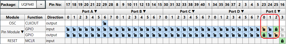
- Go to Project Resources
→ System → Pin Module and do the following configurations:
- RE2 Custom Name: SW0
- RE2 WPU: checked
- RE0 Custom Name: LED0
- RE0 Output: checked
The names used in this examples are ‘LED0’ for the RE0 pin and ‘SW0’ for the RE2 pin.
- In the Project Resources window, press the Generate button so that the MCC can generate the code capable of configuring the microcontroller as specified.
- In the
main.cfile generated by MCC, change or add the following code:while (1) { if(SW0_GetValue()) { LED0_SetHigh(); } else { LED0_SetLow(); } }
- Go to Project Resources
→ System → Pin Module and do the following configurations:

1.7.3.2 Bare Metal Code
The necessary code and functions to implement the example are analyzed in this section.
The first step is to configure the microcontroller to disable the Watchdog Timer and enable the Master Clear external pin.
#pragma config WDTE = OFF       /* disable Watchdog */
#pragma config LVP = ON         /* Low voltage programming enabled */
The main clock of the microcontroller must be initialized. The following function initializes the system clock to have as input clock the HFINTOSC oscillator and to run at 1 MHz:
static void CLK_Initialize(void)
{
    /* set HFINTOSC Oscillator */
    OSCCON1bits.NOSC = 6;
    /* set HFFRQ to 1 MHz */
    OSCFRQbits.HFFRQ = 0;
}
The peripheral initialization must be added to the project. The PORT registers allow the user to configure a pin as input or output, enable the weak pull-up and enable the digital input buffer for the desired pins.
The RE0 pin is configured as output and the RE2 pin is configured as digital input, with weak pull-up enabled. The desired configuration for this example translates to the following code:
static void PORT_Initialize(void)
{
    /* Set RE0 (LED) pin as output */
    TRISEbits.TRISE0 = 0;
    /* Set RE2 (button) pin as input*/
    TRISEbits.TRISE2 = 1;

    /* Enable weak pull-up for pin RE2 (button) */
    WPUEbits.WPUE2 = 1;

    /* Enable digital input buffer for pin RE2 (button) */
    ANSELEbits.ANSELE2 = 0;
}0’ (the button is pressed), the microcontroller will turn on the
LED by driving the output pin low. Otherwise, if the pin value is ‘1’
(the button is released), the microcontroller will turn off the LED by driving the
output pin high. This translates to the following code:
    while (1)
    {
        if(PORTEbits.RE2)     /* Read the input pin value */
        {
            LATEbits.LATE0 = 1;   /* Turn off LED */
        }
        else
        {
            LATEbits.LATE0 = 0;  /* Turn on LED */
        }
    }
1.7.4 Using GPIO Interrupts
This example consists of toggling the output pin value when an IOC is detected on the input pin. An interrupt can be generated by detecting a signal at the port pin that has either a rising or falling edge.
In this example, the interrupt is configured to be triggered on the falling edge of the
input signal (the value is changed from logic ‘1’ to logic
‘0’), in order to generate the interrupt when the button is
pressed. The interrupt routine consists of toggling the output pin value, which causes
the LED to turn on and off.
For this example, the RA0 pin is configured as input with IOC enabled on falling edge and connected to a button while the RE0 pin is configured as output and connected to an LED.
- System clock initialization
- Port initialization
- Interrupts initialization
1.7.4.1 MCC Generated Code
To generate this project using MPLAB Code Configurator (MCC), follow the next steps:
- Create a new MPLAB X IDE project for PIC18F47Q10.
- Open MCC from the toolbar (for details on how to install the MCC plug-in, see References).
- Go to Project Resources →
System → System Module and do the following configurations:
- Oscillator Select: HFINTOSC
- HF Internal Clock: Select 1_MHz
- Clock Divider: 1
- In the Watchdog Timer Enable field in WWDT tab, ensure ‘WDT Disabled’ is selected
- In the Programming tab, ensure Low-voltage Programming Enable is checked
- Open the Pin Manager → Grid View
window, select UQFN40 in the MCU package field and make the following pin
configurations:
Figure 1-50 1-51 1-52. Pin Mapping 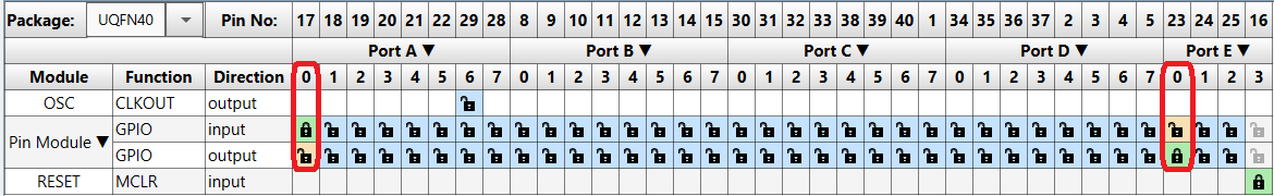
- Go to Project Resources
→ System → Pin Module → Easy Setup and do the following
configurations:
- RA0 Custom Name: RA0
- RA0 WPU: checked
- RA0 IOC: negative
- RE0 Custom Name: LED0
- RE0 Output: checked
- In the Project Resources window, press the Generate button so that the MCC can generate the code capable to configure the microcontroller as specified.
- In the
main.cfile which has been generated by MCC, change or add the following code:- Enable the global interrupts
- Add the IOC0 interrupt function
- Set the IOC0 interrupt handler initializer
static void IOC0_ISR()
{
    if(IOCAFbits.IOCAF0 == 1)
    {
        LED0_Toggle();
    }
}

void main(void)
{

    // Enable the Global Interrupts
    INTERRUPT_GlobalInterruptEnable();

    // Disable the Global Interrupts
    //INTERRUPT_GlobalInterruptDisable();

    // Enable the Peripheral Interrupts
    //INTERRUPT_PeripheralInterruptEnable();

    // Disable the Peripheral Interrupts
    //INTERRUPT_PeripheralInterruptDisable();

    IOCAF0_SetInterruptHandler(IOC0_ISR);

    while (1)
    {
        // Add your application code
    }
}
- Go to Project Resources
→ System → Pin Module → Easy Setup and do the following
configurations:
1.7.4.2 Bare Metal Code
The necessary code and functions to implement the presented example are analyzed in this section.
The first step is to configure the microcontroller to disable the Watchdog Timer and enable the Master Clear external pin.
#pragma config WDTE = OFF       /* disable Watchdog */
#pragma config LVP = ON         /* Low voltage programming enabled */
The main clock of the microcontroller must be configured. The following function initializes the system clock to have as input clock the HFINTOSC oscillator and to run at 1 MHz:
static void CLK_Initialize(void)
{
    /* set HFINTOSC Oscillator */
    OSCCON1bits.NOSC = 6;
    /* set HFFRQ to 1 MHz */
    OSCFRQbits.HFFRQ = 0;
}
For this example, the RA0 pin from PORTA is configured as an input pin and connected to a button in order to generate the desired interrupt. The PORT initialization function is listed below:
static void PORT_Initialize(void)
{
    TRISEbits.TRISE0 = 0;   /* Set RE0 pin as output (LED) */
    TRISAbits.TRISA0 = 1;   /* Set RA0 pin as input */

    ANSELAbits.ANSELA0 = 0; /* Enable Digital Input buffers for RA0 */

    WPUAbits.WPUA0 = 1;     /* Enable weak pull-up for RA0 */
}
The next step is to initialize the IOC. For this example, the IOC is configured to be triggered on the falling edge of the input signal. The code is listed below:
static void IOC_Initialize(void)
{
    IOCAFbits.IOCAF0 = 0;   /* Clear interrupt flag */

    IOCANbits.IOCAN0 = 1;   /* Enable IOC on negative change */

    PIE0bits.IOCIE = 1;     /* Enable IOC interrupt */
}
In order to work with interrupts, the user must enable the global interrupts by setting the corresponding bit in the INTCON register. The function is listed below:
static void INTERRUPT_Initialize(void)
{
    INTCONbits.GIE = 1;     /* Enable global interrupts */
}
The IOC Interrupt Service Routine (ISR) function that will be called when receiving an IOC interrupt is listed below:
static void IOC0_ISR (void)
{
    /* Clear the interrupt flag */
    IOCAFbits.IOCAF0 = 0;
    /* Toggle the LED */
    LATEbits.LATE0 = ~LATEbits.LATE0;
}
In this function, the IOC interrupt flag must be cleared and, in this instance, the output value is toggled to turn an LED on or off every time an interrupt is triggered.
An interrupt handler is needed to manage all the desired interrupts. For this example, the interrupt handler will call the IOC0_ISR interrupt routine function as listed below:
void __interrupt() INTERRUPT_InterruptManager (void)
{
    if(IOCAFbits.IOCAF0)    /* Check the interrupt flag */
    {
        IOC0_ISR();
    }
}
1.7.5 Wake-Up from Sleep
This use case presents how to put the microcontroller in Sleep mode and wake it up using the IOC. When a falling edge is detected on the input pin, the device will wake up. The exit from Sleep mode is signaled using an LED. If the microcontroller wakes up, it will turn the LED on, keep the LED on for 100 ms and then turn it off. The Sleep mode is used to provide power efficiency.
For this example, the RA0 pin is configured as input with IOC enabled on falling edge and connected to a button while the RE0 pin is configured as output and connected to an LED.
- System clock initialization
- Port initialization
- Interrupts initialization
1.7.5.1 MCC Generated Code
- Create a new MPLAB X IDE project for PIC18F47Q10.
- Open MCC from the toolbar (for details on how to install the MCC plug-in, see References).
- Go to Project Resources →
System → System Module and do the following configurations:
- Oscillator Select: HFINTOSC
- HF Internal Clock: Select 1_MHz
- Clock Divider: 1
- In the Watchdog Timer Enable field in WWDT tab, ensure ‘WDT Disabled’ is selected
- In the Programming tab, ensure Low-voltage Programming Enable is checked
- Open the Pin Manager → Grid View
window, select UQFN40 in the MCU package field, and make the following pin
configurations:
Figure 1-50 1-51 1-52. Pin Mapping
- Go to Project Resources
→ System → Pin Module → Easy Setup and do the following
configurations:
- RA0 Custom Name: RA0
- RA0 WPU: checked
- RA0 IOC: negative
- RE0 Custom Name: LED0
- RE0 Output: checked
- In the Project Resources window, press the Generate button so that the MCC can generate the code capable of configuring the microcontroller as specified.
- In the
main.cfile generated by MCC, add the following code:- Enable the global interrupts
- Add the IOC0 interrupt function
- Set the IOC0 interrupt handler initializer
- Put the device in Sleep
#define DELAY_MS 100

static void IOC0_ISR()
{
    if(IOCAFbits.IOCAF0 == 1)
    {
        ;
    }
}

void main(void)
{
    // Initialize the device
    SYSTEM_Initialize();

    // Enable the Global Interrupts
    INTERRUPT_GlobalInterruptEnable();

    // Disable the Global Interrupts
    //INTERRUPT_GlobalInterruptDisable();

    // Enable the Peripheral Interrupts
    //INTERRUPT_PeripheralInterruptEnable();

    // Disable the Peripheral Interrupts
    //INTERRUPT_PeripheralInterruptDisable();

    IOCAF0_SetInterruptHandler(IOC0_ISR);

    while (1)
    {
        LED0_SetLow();
        __delay_ms(DELAY_MS);
        LED0_SetHigh();

        SLEEP();
    }
}
- Go to Project Resources
→ System → Pin Module → Easy Setup and do the following
configurations:
1.7.5.2 Bare Metal Code
The necessary code and functions to implement the presented example are analyzed in this section.
The first step is to configure the microcontroller to disable the Watchdog Timer and enable the Master Clear external pin.
#pragma config WDTE = OFF       /* disable Watchdog */
#pragma config LVP = ON         /* Low voltage programming enabled */
The _XTAL_FREQ macro needs to be defined in order to use
the __delay_ms function. Also, the _XTAL_FREQ value
must be the same as the system clock.
#define _XTAL_FREQ 1000000ULThe main clock of the microcontroller must be configured. The following function initializes the system clock to have as input clock the HFINTOSC oscillator and to run at 1 MHz:
static void CLK_Initialize(void)
{
    /* set HFINTOSC Oscillator */
    OSCCON1bits.NOSC = 6;
    /* set HFFRQ to 1 MHz */
    OSCFRQbits.HFFRQ = 0;
}
For this example, the RA0 pin from PORTA is configured as a digital input and connected to a button in order to generate the desired interrupt. The RE0 pin is configured as output and connected to an LED. The PORT initialization function is listed below:
static void PORT_Initialize(void)
{
    TRISEbits.TRISE0 = 0;   /* Set RE0 pin as output (LED) */
    TRISAbits.TRISA0 = 1;   /* Set RA0 pin as input */

    ANSELAbits.ANSELA0 = 0; /* Enable Digital Input buffers for RA0 */

    WPUAbits.WPUA0 = 1;     /* Enable weak pull-up for RA0 */
}
The next step is to initialize the IOC. For this example, the IOC is configured to be triggered on the falling edge of the input signal. The code is listed below:
static void IOC_Initialize(void)
{
    IOCAFbits.IOCAF0 = 0;   /* Clear interrupt flag */

    IOCANbits.IOCAN0 = 1;   /* Enable IOC on negative change */

    PIE0bits.IOCIE = 1;     /* Enable IOC interrupt */
}
In order to work with interrupts, the users must add an interrupt initialization function that activates the global and the peripheral interrupts. The function is listed below.
static void INTERRUPT_Initialize(void)
{
    INTCONbits.GIE = 1;     /* Enable global interrupts */
}
The IOC ISR function that will be called when receiving an IOC interrupt is listed below: In this function, the only action needed in this example is to clear the interrupt flag.
static void IOC0_ISR (void)
{
    IOCAFbits.IOCAF0 = 0;   /* Clear the interrupt flag */
}
In this function, the only action needed in this example is to clear the interrupt flag.
An interrupt handler is needed to manage all the desired interrupts. For this example, the interrupt handler will call the IOC0_ISR interrupt routine function, as listed below:
void __interrupt() INTERRUPT_InterruptManager (void)
{
    if(IOCAFbits.IOCAF0)    /* Check the interrupt flag */
    {
        IOC0_ISR();
    }
}
Additionally, for this example, the users must add the LED blinking
functionality in the while(1) loop. After turning the LED on and off,
the device enters Sleep mode.
    while(1)
    {
        /* Turn the LED on*/
        LATEbits.LATE0 = 0;
        __delay_ms(DELAY_MS);
        /* Turn the LED off*/
        LATEbits.LATE0 = 1;

        SLEEP();
    }