
1.3 Getting Started with SPI
1.3.1 Introduction
| Author: Iustinian Bujor, Microchip Technology Inc. |
The approach in implementing the SPI communication protocol is different among the PIC18F device family of microcontrollers. While the PIC18-K40 and PIC18-Q10 product families have a Master Synchronous Serial Port (MSSP) peripheral, the PIC18-K42, PIC18-K83, PIC18-Q41, PIC18-Q43 and PIC18-Q84 product families have a dedicated Serial Peripheral Interface (SPI) peripheral.
Both peripherals are serial interfaces useful for communicating with other peripherals or microcontroller devices, but there are also differences between them. The MSSP peripheral can operate in one of two modes: Serial Peripheral Interface (SPI) and Inter-Integrated Circuit (I2C), which allows the advantage of implementing both communication protocols with the same hardware. The dedicated SPI peripheral works similarly to the MSSP, and has more features, such as Receive Only and Transmit Only modes, Double Buffering and Receive and Transmit FIFO.
This technical brief provides information about MSSP on the PIC18-K40 and PIC18-Q10 product families and intends to familiarize the user with PIC® microcontrollers.
The document describes the application area, the modes of operation and the hardware and software requirements of the MSSP module configured in SPI mode.
Throughout the document, the configuration of the peripheral will be described in detail, starting with the location of the SPI pins, the direction of the pins, how to initialize the device as a Host or a Client and how to exchange data inside the system. This document covers the following use cases:
- Sending Data
as a Host SPI Device with Multiple Clients:
This example shows how to configure the device as a Host to control two Client devices and to send data using the polling method.
- Receiving
Data as a Client SPI Device:
This example shows how to configure the device as a Client that will wait for the incoming data using the polling method.
- Exchanging
Data as a Client SPI Device Using Interrupts:
This example shows how to configure the device as a Client that will wait for the incoming data. In this case, the data transmission/reception will be triggered by interrupts.
- Changing Data
Transfer Type:
This example shows how to configure the device as a Host that will send data with respect to the clock polarity and the clock edge.
For each use case, there are three different implementations, which have the same functionalities: one code generated with MPLAB® Code Configurator (MCC), one code generated using Foundation Services Library and one bare metal code.
The MCC generated code offers hardware abstraction layers that ease the use of the code across different devices from the same family. Also, MCC provides a graphical interface that eases the peripheral configuration process and helps the users to evaluate the peripherals they are not familiar with. The Foundation Services generated code offers a driver-independent Application Programming Interface (API) and facilitates the portability of code across different platforms. The bare metal code tends to be more device specific, allowing a fast ramp-up on the use case associated code.

1.3.2 Peripheral Overview
The SPI bus is a synchronous serial data communication bus that operates in Full Duplex mode, using a channel for transmitting and another channel for receiving data. The devices communicate in a master-slave environment, with a single master at a time and one or more slaves.
The SPI bus consists of four signal connections:
- SCK: Serial Clock (output from master)
- SDO: Serial Data Out (data output)
- SDI: Serial Data Input (data input)
- SS: Slave Select (active-low, output from master)
The master device is the only one that can generate a clock. Therefore, it is typically the initiator of the data exchange, although there are methods of slave initiation. The SPI master device uses the same SCK, SDO and SDI channels for all the slaves, but usually individual lines of SS for each of the slaves. However, the daisy-chain feature offers the possibility of using only one SS line to control more than one slave device. The master device selects the desired slave by pulling the SS signal low.
The data to be sent will be stored in the buffer register (SSPxBUF). The master device transmits information out on its SDO output pin, which is connected to and received by the slave’s SDI input pin. The slave device transmits information out on its SDO output pin, which is connected to and received by the master’s SDI input pin.
Transmissions involve two eight bit-sized shift registers, one in the master and the other in the slave. With either the master or the slave device, data is always shifted out one bit at a time, on the programmed clock edge and with the Most Significant bit (MSb) shifted out first. At the same time, a new Least Significant bit (LSb) is shifted into the same register.
Any write to the SSPxBUF register during transmission/reception of data will be ignored and the Write Collision Detect (WCOL) bit from the MSSP Control 1 (SSPxCON1) register will be set. User software must clear the WCOL bit to allow the following write(s) to the SSPxBUF register to complete successfully. The MSSP Shift register (SSPSR) is not directly readable or writable and can only be accessed by addressing the SSPxBUF register.

The data transfer type represents the way in which data are transmitted with respect to the clock generation. The clock polarity and the clock edge are the important parameters for data modes.
The clock polarity refers to the level of the signal in Idle state. The signal can be either low in Idle state, and start with a rising edge when transmitting data, or high in Idle state and start with a falling edge when transmitting data. Depending on the edge, the data are transmitted with respect to the clock on the channel and, therefore, either on a rising or falling edge.
For a better understanding, see the following figure:

1.3.3 Sending Data as a Master SPI Device with Multiple Slaves
The master is the device that decides when to trigger communication and which slave is the recipient of the message. SPI master devices are generally used in high-speed communication and the focus is to exchange data with other devices acting as slaves (e.g., sensors, memories, or other microcontrollers).
This use case presents how to configure the SPI as a master device along with its pins to send data to two slave devices, one at a time.
- System clock initialization
- SPI1 initialization
- Peripheral Pin Selection (PPS) initialization
- Port initialization
- Slave control functions
- Data exchange function
1.3.3.1 MCC Generated Code
To generate this project using MPLAB® Code Configurator (MCC), follow the next steps:
- Create a new MPLAB X IDE project for PIC18F47Q10.
- Open the MCC from the toolbar. Information about how to install the MCC plug-in can be found here.
- Go to Project Resources →
System → System Module and do the following configuration:
- Oscillator Select: HFINTOSC
- HF Internal Clock: 64_MHz
- Clock Divider: 1
- In the Watchdog Timer Enable field in the WWDT tab, make sure WDT Disabled is selected.
- In the Programming tab, make sure Low-Voltage Programming Enable is checked.
- From the Device Resources window, add
MSSP1 and do the following configuration:
- Serial Protocol: SPI
- Mode: Master
- SPI Mode: SPI Mode 0
- Input Data Sampled At: Middle
- Clock Source Selection: FOSC/4_SSPxADD
- SPI Clock Frequency box: 8000000
- Open Pin Manager → Grid
View window, select UQFN40 in the Package field and do the
following pin configurations:
- Set Port C pin 6 (RC6) as output for Slave Select 1 (SS1)
- Set Port C pin 7 (RC7) as output for Slave Select 2 (SS2)
Figure 1-18. Pin Mapping 
- Click Pin Module in the
Project Resources tab and set custom names for the SS pins:
- Rename RC6 to Slave1
- Rename RC7 to Slave2
- Click Generate in the Project Resources tab.
- In the
main.cfile which has been generated by MCC, change or add the following code:- Control of slave devices
- Data transmission
uint8_t writeData = 1;          /* Data that will be transmitted */
uint8_t receiveData;            /* Data that will be received */

void main(void)
{
    // Initialize the device
    SYSTEM_Initialize();

    while (1)
    {
        SPI1_Open(SPI1_DEFAULT);
        Slave1_SetLow();
        receiveData = SPI1_ExchangeByte(writeData);
        Slave1_SetHigh();
        SPI1_Close();

        SPI1_Open(SPI1_DEFAULT);
        Slave2_SetLow();
        receiveData = SPI1_ExchangeByte(writeData);
        Slave2_SetHigh();
        SPI1_Close();
    }
}

1.3.3.2 Foundation Services Generated Code
To generate this project using Foundation Services Library, follow the next steps:
- Create a new MPLAB X IDE project for PIC18F47Q10.
- Open the MCC from the toolbar. Information on how to install the MCC plug-in can be found here.
- Go to Project Resources →
System → System Module and do the following configuration:
- Oscillator Select: HFINTOSC
- HF Internal Clock: 64_MHz
- Clock Divider: 1
- In the Watchdog Timer Enable field in the WWDT tab, make sure WDT Disabled is selected.
- In the Programming tab, make sure Low-Voltage Programming Enable is checked.
- From the Device Resources →
Foundation Services window, add SPIMASTER and do the following
configuration:
- Name: MASTER0
- SPI Mode: MODE0
- SPI Data Input Sample: MIDDLE
- Speed (kHz): 8000
- SPI: MSSP1
- Open Pin Manager → Grid
View window, select UQFN40 in the Package field and do the
following pin configurations:
- Set Port C pin 6 (RC6) as output for Slave Select 1 (SS1)
- Set Port C pin 7 (RC7) as output for Slave Select 2 (SS2)
Figure 1-19. Pin Mapping
- Click Pin Module in the
Project Resources tab and set custom names for the SS pins:
- Rename RC6 to Slave1
- Rename RC7 to Slave2
- Click Generate in the Project Resources tab.
- In the
main.cfile that has been generated using Foundation Services Library, add the following code:- Control of slave devices
- Data transmission
uint8_t writeData = 1;          /* Data that will be transmitted */
uint8_t receiveData;            /* Data that will be received */

void main(void)
{
    // Initialize the device
    SYSTEM_Initialize();

    while (1)
    {
        spi_master_open(MASTER0);
        Slave1_SetLow();
        receiveData = SPI1_ExchangeByte(writeData);
        Slave1_SetHigh();
        SPI1_Close();

        spi_master_open(MASTER0);
        Slave2_SetLow();
        receiveData = SPI1_ExchangeByte(writeData);
        Slave2_SetHigh();
        SPI1_Close();
    }
}
1.3.3.3 Bare Metal Code
The necessary code and functions to implement the presented example are analyzed in this section.
The first step will be to configure the microcontroller to disable the Watchdog Timer and to enable Low-Voltage Programming.
#pragma config WDTE = OFF
#pragma config LVP = ON
The internal oscillator has to be set to the desired value. This example uses the HFINTOSC with a frequency of 64 MHz. This translates into the following function:
static void CLK_Initialize(void)
{
    OSCCON1bits.NOSC = 6;        /* HFINTOSC Oscillator */

    OSCFRQbits.HFFRQ = 8;        /* HFFRQ 64 MHz */
}
The SPI clock frequency is derived from the main clock of the microcontroller (OSCFRQ) and is reduced using a prescaler or a divider circuit present in the MSSP hardware.
Configure the MSSP in SPI Master mode, with the previous selected clock source. An 8 MHz frequency will result in configuring the device in SPI Master mode with SPI clock = FOSC / (4*(SSP1ADD + 1)). This translates into the following code:
static void SPI1_Initialize(void)
{
    SSP1ADD = 0x01;     /* SSP1ADD = 1 */

    SSP1CON1 = 0x2A;    /* Enable module, SPI Master Mode */
}
Configuring the location of the pins is independent of the application purpose and the SPI mode. Each microcontroller has its own default physical pin position for peripherals, but the pin positions can be changed using the Peripheral Pin Select (PPS).
The SPI pins can be relocated using the SSPxCLKPPS, SSPxDATPPS and SSPxSSPPS registers for the input channels. Use the RxyPPS registers for the output channels.
The PPS configuration values can be found in the Peripheral Pin Select Module section of a device data sheet. For SPI1 in Master mode, only the SDI pin requires input and use it with its default location RC4. SCK was mapped to RC3 and SDO was mapped to RC5. This translates into the following code:
static void PPS_Initialize(void)
{
    RC3PPS = 0x0F;               /* SCK channel on RC3 */

    SSP1DATPPS = 0x14;           /* SDI channel on RC4 */

    RC5PPS = 0x10;               /* SDO channel on RC5 */
}
Since the master sends data to two slave devices, two SS pins are needed (SS1 and SS2) in this example. For both of them, a General Purpose Input/Output (GPIO) pin was used (RC6 for SS1 and RC7 for SS2).
| Channel | Pin |
|---|---|
| SCK | RC3 |
| SDI | RC4 |
| SDO | RC5 |
| SS1 | RC6 |
| SS2 | RC7 |
Because the master devices control and initiate transmissions, the SDO, SCK and SS pins must be configured as output while the SDI channel will keep its default direction as input. The following example is based on the relocation of the SPI1 pins made above:
static void PORT_Initialize(void)
{
    /* SDI as input; SCK, SDO, SS1, SS2 as output */
    TRISC = 0x17;

    /* SCK, SDI, SDO, SS1, SS2 as digital pins */
    ANSELC = 0x07;
}
A master will control a slave by pulling the SS pin low. If the slave has set the direction of its SDO pin to output when the SS pin is low, the SPI driver of the slave will take control of the SDI pin of the master. This will shift data out from its Transmit Buffer register.
All slave devices can receive a message, but only those with the SS pin pulled low can send data back. It is not recommended to enable more than one slave in a typical connection since all of them will try to respond to the message. With the master having only one SDI channel, the transmission will result in a write collision.
Before sending data, the user must pull one of the configured SS signals low to let the correspondent slave device know it is the recipient of the message.
static void SPI1_slave1Select(void)
{
    LATCbits.LATC6 = 0;          /* Set SS1 pin value to LOW */
}
Once the user writes new data into the Buffer register, the hardware starts a new transfer. This will generate the clock on the line and shift out the bits. The bits are shifted out starting with the Most Significant bit (MSb).
When the hardware finishes shifting all the bits, it sets the Buffer Full Status bit. The user must check the state of the flag before writing new data into the register by constantly reading the value of the bit (polling). If polling is not done, a write collision will occur.
static uint8_t SPI1_exchangeByte(uint8_t data)
{
    SSP1BUF = data;

    while(!PIR3bits.SSP1IF)     /* Wait until data is exchanged */
    {
        ;
    }
    PIR3bits.SSP1IF = 0;

    return SSP1BUF;
}
The user can pull the SS channel high if there is nothing left to transmit.
static void SPI1_slave1Deselect(void)
{
    LATCbits.LATC6 = 1;          /* Set SS1 pin value to HIGH */
}
The selection of the slave devices and the data transmission are done in the main function.
int main(void)
{
    CLK_Initialize();
    PPS_Initialize();
    PORT_Initialize();
    SPI1_Initialize();

    while(1)
    {
        SPI1_slave1Select();
        receiveData = SPI1_exchangeByte(writeData);
        SPI1_slave1Deselect();

        SPI1_slave2Select();
        receiveData = SPI1_exchangeByte(writeData);
        SPI1_slave2Deselect();
    }
}
1.3.4 Receiving Data as a Slave SPI Device
The slave devices are represented by actuators, sensors, external memories, display drivers and more. Slaves usually do not initiate any action; they only act whenever the master initiates. Although there are cases when slave devices can initiate a transmission, their behavior in such a scenario is not presented in this use case. A slave must always be available and has to wait until the master pulls its SS channel low.
This use case presents how to configure the SPI as a slave device, along with its pins to receive data from a master device.
- System clock initialization
- SPI1 initialization
- PPS initialization
- Port initialization
- Polling check
- Data exchange function
1.3.4.1 MCC Generated Code
To generate this project using MPLAB® Code Configurator (MCC), follow the next steps:
- Create a new MPLAB X IDE project for PIC18F47Q10.
- Open MCC from the toolbar. Information on how to install the MCC plug-in can be found here.
- Go to Project Resources →
System → System Module and do the following configuration:
- Oscillator Select: HFINTOSC
- HF Internal Clock: 64_MHz
- Clock Divider: 1
- In the Watchdog Timer Enable field in the WWDT tab, make sure WDT Disabled is selected.
- In the Programming tab, make sure Low-Voltage Programming Enable is checked.
- From the Device Resources window, add
MSSP1 and do the following configuration:
- Serial Protocol: SPI
- Mode: Slave
- SPI Mode: SPI Mode 0
- Enable Slave Select: checked
- Open Pin Manager → Grid
View window and select UQFN40 in the Package field. The SCK,
SDO, SDI and SS pins appear alongside the MSSP1 peripheral and have their direction
preset.
Figure 1-20. Pin Mapping 
- Click Generate in the Project Resources tab.
- In the
main.cfile which has been generated by MCC, change or add the following code:- Peripheral initialization
- Data receiving
uint8_t receiveData;        /* Data that will be received */
uint8_t writeData = 1;      /* Data that will be transmitted */

void main(void)
{
    // Initialize the device
    SYSTEM_Initialize();

    SPI1_Open(SPI1_DEFAULT);

    while (1)
    {
        if(!RA5_GetValue())                /* SS line is LOW */
        {
            receiveData = SPI1_ExchangeByte(writeData);
        }
    }
}
1.3.4.2 Foundation Services Generated Code
To generate this project using Foundation Services Library, follow the next steps:
- Create a new MPLAB X IDE project for PIC18F47Q10.
- Open MCC from the toolbar. Information about how to install the MCC plug-in can be found here.
- Go to Project Resources →
System → System Module and do the following configuration:
- Oscillator Select: HFINTOSC
- HF Internal Clock: 64_MHz
- Clock Divider: 1
- In the Watchdog Timer Enable field in the WWDT tab, make sure WDT Disabled is selected.
- In the Programming tab, make sure Low-Voltage Programming Enable is checked.
- From the Device Resources →
Foundation Services window, add SPISLAVE and do the following
configuration:
- Name: SLAVE0
- SPI Mode: MODE0
- SPI: MSSP1
- Go to Project Resources → System → Interrupt Module → Easy Setup and uncheck the box right next to Pin Module.
- Open Pin Manager → Grid
View window, select UQFN40 in the Package field and do the
following pin configuration:
- Set Port A pin 5 (RA5) as input for Slave Select (SS)
Figure 1-21 1-23 1-25. Pin Mapping 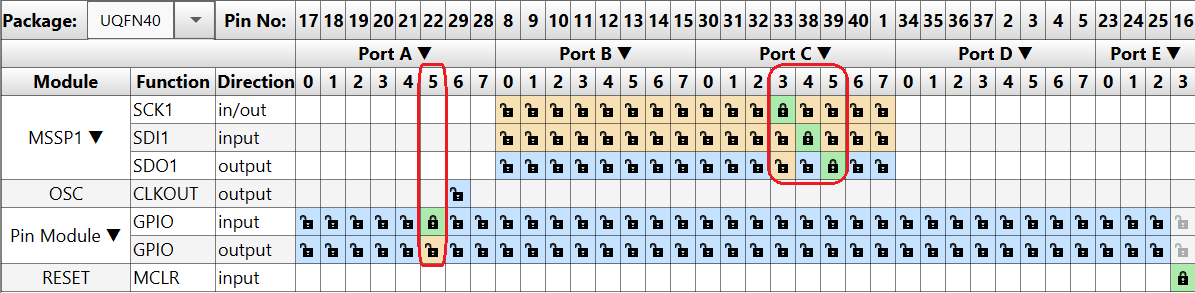
- Click Generate in the Project Resources tab.
- In the
main.cfile which has been generated using Foundation Services Library, add the following code:- Peripheral initialization
- Data receiving
uint8_t receiveData;        /* Data that will be received */
uint8_t writeData = 1;      /* Data that will be transmitted */

void main(void)
{
    // Initialize the device
    SYSTEM_Initialize();

    spi1_open(SLAVE0_CONFIG);

    while (1)
    {
        if(!SS_GetValue())                /* SS line is LOW */
        {
            receiveData = spi1_exchangeByte(writeData);
        }
    }
}
1.3.4.3 Bare Metal Code
The necessary code and functions to implement the presented example are analyzed in this section.
The first step will be to configure the microcontroller to disable the Watchdog Timer and to enable Low-Voltage Programming.
#pragma config WDTE = OFF
#pragma config LVP = ON
The internal oscillator has to be set to the desired value. This example uses the HFINTOSC with a frequency of 64 MHz, which translates into the following function:
static void CLK_Initialize(void)
{
    OSCCON1bits.NOSC = 6;        /* HFINTOSC Oscillator */

    OSCFRQbits.HFFRQ = 8;        /* HFFRQ 64 MHz */
}
Since the slave gets its clock signal from the master device, there is no point in changing the clock divider of the peripheral. This change will have no effect in SPI Slave mode. However, the hardware peripheral has to sample the data received on their SDI channel. For the data signal to be correctly reconstructed, the main clock frequency of the device must be at least double the frequency received on the SPI SCK channel.
Next is an example on how to configure the MSSP in SPI Slave mode.
static void SPI1_Initialize(void)
{
    /* Enable module, SPI Slave Mode */
    SSP1CON1 = 0x24;
}
Configuring the location of the pins is independent of the application purpose and the SPI mode. Each microcontroller has its own default physical pin position for peripherals, but the pin positions can be changed using the Peripheral Pin Select (PPS).
The SPI pins can be relocated using the SSPxCLKPPS, SSPxDATPPS and SSPxSSPPS registers for the input channels. Use the RxyPPS registers for the output channels.
The PPS configuration values can be found in the Peripheral Pin Select Module section of a device data sheet. For SPI1 in Slave mode, the SDI and SS pins require input, so use them with their default locations (RC4 for SDI and RA5 for SS). SCK was mapped to RC3 and SDO was mapped to RC5 in this example. This translates into the following code:
static void PPS_Initialize(void)
{
    SSP1SSPPS = 0x05;             /* SS channel on RA5 */

    RC3PPS = 0x0F;                /* SCK channel on RC3 */

    SSP1DATPPS = 0x14;            /* SDI channel on RC4 */

    RC5PPS = 0x10;                /* SDO channel on RC5 */
}
| Channel | Pin |
|---|---|
| SS | RA5 |
| SCK | RC3 |
| SDI | RC4 |
| SDO | RC5 |
Since the slave device receives the incoming transmissions, the SDI, SCK and SS will keep their default direction as input while the SDO channel must be configured as output. The following example is based on the relocation of the SPI1 pins made above:
static void PORT_Initialize(void)
{
    /* SDO as output; SDI, SCK as input */
    TRISC = 0xDF;

    /* SS as digital pin */
    ANSELA = 0xDF;

    /* SCK, SDI, SDO as digital pins */
    ANSELC = 0xC7;
}
All the slave devices connected to the SPI bus will receive the message sent on their SDI channel by the master device. A slave cannot respond to a message unless the SS channel is pulled low. When the master device pulls the SS pin low, the SPI peripheral of the slave device will take control of its SDO pin and will shift data out.
Checking the value of SS is done through the polling method.
if(!PORTAbits.RA5) /* SS line is LOW */
The peripheral will signal the reception of a new data by activating the SSPxIF flag of the PIR3 register. The user has to check the value of the bit also through polling.
After the received data was processed as wanted, the flag needs to be cleared.
This is done by writing a ‘1’ in the bit location.
static uint8_t SPI1_exchangeByte(uint8_t data)
{
    SSP1BUF = data;

    while(!PIR3bits.SSP1IF) /* Wait until data is exchanged */
    {
        ;
    }
    PIR3bits.SSP1IF = 0;

    return SSP1BUF;
}
The checking of the SS line and the data receiving is done in the main function.
int main(void)
{
    CLK_Initialize();
    PPS_Initialize();
    PORT_Initialize();
    SPI1_Initialize();

    while(1)
    {
        if(!PORTAbits.RA5)              /* SS line is LOW */
        {
            receiveData = SPI1_exchangeByte(writeData);
        }
    }
}
1.3.5 Exchanging Data as a Slave SPI Device Using Interrupts
The slave devices are represented by actuators, sensors, external memories, display drivers and more. Slaves usually do not initiate any action; they only act whenever the master initiates. Although there are cases when slave devices can initiate a transmission, their behavior in this scenario is not presented in this use case.
This use case presents how to configure the SPI as a slave device, along with its pins to exchange data with a master device. The data received will be interrupt driven.
- System clock initialization
- SPI1 initialization
- PPS initialization
- Port initialization
- Interrupts initialization
- Data exchange function
- SPI1 interrupt handling
1.3.5.1 MCC Generated Code
To generate this project using MPLAB® Code Configurator (MCC), follow the next steps:
- Create a new MPLAB X IDE project for PIC18F47Q10.
- Open MCC from the toolbar. Information about how to install the MCC plug-in can be found here.
- Go to Project Resources →
System → System Module and do the following configuration:
- Oscillator Select: HFINTOSC
- HF Internal Clock: 64_MHz
- Clock Divider: 1
- In the Watchdog Timer Enable field in the WWDT tab, make sure WDT Disabled is selected.
- In the Programming tab, make sure Low-Voltage Programming Enable is checked.
- From the Device Resources window, add
MSSP1 and do the following configuration:
- Hardware Settings
tab
- Serial Protocol: SPI
- Mode: Slave
- SPI Mode: SPI Mode 0
- Enable Slave Select: checked
- Interrupt Settings
tab
- Enable SPI Interrupt: checked
- Hardware Settings
tab
- Open Pin Manager → Grid
View window and select UQFN40 in the Package field. The SCK,
SDO, SDI and SS pins appear alongside the MSSP1 peripheral and have their direction
preset.
Figure 1-22 1-24. Pin Mapping
- Click Generate in the Project Resources tab.
- In the
main.cfile which has been generated by MCC, change or add the following code:- Enable the global and peripheral interrupts
- Add the MSSP1 interrupt function
- Set the MSSP1 interrupt handler initialize
static void MSSP1_interruptHandler(void);

volatile uint8_t receiveData;        /* Data that will be received */
volatile uint8_t writeData = 1;      /* Data that will be transmitted */

static void MSSP1_interruptHandler(void)
{
    receiveData = SPI1_ExchangeByte(writeData);
}

void main(void)
{
    // Initialize the device
    SYSTEM_Initialize();

    SPI1_Open(SPI1_DEFAULT);

    SPI1_SetInterruptHandler(MSSP1_interruptHandler);

    // Enable the Global Interrupts
    INTERRUPT_GlobalInterruptEnable();

    // Disable the Global Interrupts
    //INTERRUPT_GlobalInterruptDisable();

    // Enable the Peripheral Interrupts
    INTERRUPT_PeripheralInterruptEnable();

    // Disable the Peripheral Interrupts
    //INTERRUPT_PeripheralInterruptDisable();

    while (1)
    {
        ;
    }
}
1.3.5.2 Foundation Services Generated Code
To generate this project using Foundation Services Library, follow the next steps:
- Create a new MPLAB X IDE project for PIC18F47Q10.
- Open MCC from the toolbar. Information about how to install the MCC plug-in can be found here.
- Go to Project
Resources → System → System Module and do
the following configuration:
- Oscillator Select: HFINTOSC
- HF Internal Clock: 64_MHz
- Clock Divider: 1
- In the Watchdog Timer Enable field in the WWDT tab, make sure WDT Disabled is selected.
- In the Programming tab, make sure Low-Voltage Programming Enable is checked.
- From the Device
Resources → Foundation Services window, add
SPISLAVE and do the following configuration:
- Name: SLAVE0
- SPI Mode: MODE0
- SPI: MSSP1
- Go to Project Resources → System → Interrupt Module → Easy Setup. Uncheck the box right next to Pin Module and check the box right next to MSSP1-SSPI.
- Open Pin Manager →
Grid View window, select UQFN40 in
the Package field and do the following pin configuration:
- Set Port A pin 5 (RA5) as input for Slave Select (SS)
Figure 1-21 1-23 1-25. Pin Mapping
- Click Generate in the Project Resources tab.
- In the
main.cfile which has been generated using Foundation Services Library, add the following code:- Enable the global and peripheral interrupts
- Add the MSSP1 interrupt function
- Set the MSSP1 interrupt handler initialize
static void MSSP1_interruptHandler(void);

volatile uint8_t receiveData;        /* Data that will be received */
volatile uint8_t writeData = 1;      /* Data that will be transmitted */

static void MSSP1_interruptHandler(void)
{
    receiveData = spi1_exchangeByte(writeData);
}

void main(void)
{
    // Initialize the device
    SYSTEM_Initialize();

    spi_slave_init();

    spi1_setSpiISR(MSSP1_interruptHandler);

    // Enable the Global Interrupts
    INTERRUPT_GlobalInterruptEnable();

    // Disable the Global Interrupts
    //INTERRUPT_GlobalInterruptDisable();

    // Enable the Peripheral Interrupts
    INTERRUPT_PeripheralInterruptEnable();

    // Disable the Peripheral Interrupts
    //INTERRUPT_PeripheralInterruptDisable();

    while (1)
    {
        ;
    }
}
1.3.5.3 Bare Metal Code
The necessary code and functions to implement the presented example are analyzed in this section.
The first step will be to configure the microcontroller to disable the Watchdog Timer and to enable Low-Voltage Programming.
#pragma config WDTE = OFF
#pragma config LVP = ON
The internal oscillator has to be set to the desired value. This example uses the HFINTOSC with a frequency of 64 MHz, which translates into the following function:
static void CLK_Initialize(void)
{
    OSCCON1bits.NOSC = 6;        /* HFINTOSC Oscillator */

    OSCFRQbits.HFFRQ = 8;        /* HFFRQ 64 MHz */
}
Since the slave gets its clock signal from the master device, there is no point in changing the clock divider of the peripheral. This change will have no effect in SPI Slave mode. However, the hardware peripheral has to sample the data received on their SDI channel. For the data signal to be correctly reconstructed, the main clock frequency of the device must be at least double the clock frequency received on the SPI SCK channel.
Configure the MSSP in SPI Slave mode. To receive data using interrupts, the Interrupt Enable bit (SSPxIE) of the PIE3 register must be set.
static void SPI1_Initialize(void)
{
    /* Enable module, SPI Slave Mode */
    SSP1CON1 = 0x24;

    /* Enable MSSP interrupts */
    PIE3bits.SSP1IE = 1;
}
This allows the SPI module to trigger an interrupt every time it has received data on its SDI pin.
Configuring the location of the pins is independent of the application purpose and the SPI mode. Each microcontroller has its own default physical pin position for peripherals, but the pin positions can be changed using the Peripheral Pin Select (PPS).
The SPI pins can be relocated by using the SSPxCLKPPS, SSPxDATPPS and SSPxSSPPS registers for the input channels. Use the RxyPPS registers for the output channels.
The PPS configuration values can be found in the Peripheral Pin Select Module section of a device data sheet. For SPI1 in Slave mode, the SDI and SS pins require input, so use them with their default location (RC4 for SDI and RA5 for SS). SCK was mapped to RC3 and SDO was mapped to RC5 in this example. This translates into the following code:
static void PPS_Initialize(void)
{
    SSP1SSPPS = 0x05;             /* SS channel on RA5 */

    RC3PPS = 0x0F;                /* SCK channel on RC3 */

    SSP1DATPPS = 0x14;            /* SDI channel on RC4 */

    RC5PPS = 0x10;                /* SDO channel on RC5 */
}
| Channel | Pin |
|---|---|
| SS | RA5 |
| SCK | RC3 |
| SDI | RC4 |
| SDO | RC5 |
Since the slave device receives the incoming transmissions, the SDI, SCK and SS will keep their default direction as input while the SDO channel must be configured as output. The following example is based on the relocation of the SPI1 pins made above:
static void PORT_Initialize(void)
{
    /* SDO as output; SDI, SCK as input */
    TRISC = 0xDF;

    /* SS as digital pin */
    ANSELA = 0xDF;

    /* SCK, SDI, SDO as digital pins */
    ANSELC = 0xC7;
}
Before any transfer of data, the interrupts of the microcontroller must be activated. This is done by setting the Global Interrupt Enable (GIE) and the Peripheral Interrupt Enable (PIE) bits of the INTCON register.
static void INTERRUPT_Initialize(void)
{
    INTCONbits.GIE = 1;              /* Enable Global Interrupts */
    INTCONbits.PEIE = 1;             /* Enable Peripheral interrupts */
}
The code snippet below shows how to write to the Buffer register, clear the Interrupt flag and read the received data. The user can choose what to do with the received data and what to write back to the master:
static uint8_t SPI1_exchangeByte(uint8_t data)
{
    SSP1BUF = data;

    while(!PIR3bits.SSP1IF) /* Wait until data is exchanged */
    {
        ;
    }
    PIR3bits.SSP1IF = 0;

    return SSP1BUF;
}
This exchange function is integrated in the interrupt handler of the MSSP1.
static void MSSP1_interruptHandler(void)
{
    receiveData = SPI1_exchangeByte(writeData);
}
The interrupt handler is handled by the interrupt manager.
void __interrupt() INTERRUPT_InterruptManager(void)
{
    if(INTCONbits.PEIE == 1)
    {
        if(PIE3bits.BCL1IE == 1 && PIR3bits.BCL1IF == 1)
        {
            MSSP1_InterruptHandler();
        }
        else if(PIE3bits.SSP1IE == 1 && PIR3bits.SSP1IF == 1)
        {
            MSSP1_InterruptHandler();
        }
    }
}
1.3.6 Changing Data Transfer Type
This use case presents how to configure the SPI as a master device along with its pins to send data to a slave device in Data Mode 3.
In this mode, the Idle clock state is high and the data are transmitted on a falling edge of the clock signal (from high to low).
- System clock initialization
- SPI1 initialization
- PPS initialization
- Port initialization
- Slave control functions
- Data exchange function
1.3.6.1 MCC Generated Code
To generate this project using MPLAB® Code Configurator (MCC), follow the next steps:
- Create a new MPLAB X IDE project for PIC18F47Q10.
- Open MCC from the toolbar. Information about how to install the MCC plug-in can be found here.
- Go to Project Resources →
System → System Module and do the following configuration:
- Oscillator Select: HFINTOSC
- HF Internal Clock: 64_MHz
- Clock Divider: 1
- In the Watchdog Timer Enable field in the WWDT tab, make sure WDT Disabled is selected.
- In the Programming tab, make sure Low-Voltage Programming Enable is checked.
- From the Device Resources window, add
MSSP1 and do the following configuration:
- Serial Protocol: SPI
- Mode: Master
- SPI Mode: SPI Mode 3
- Input Data Sampled At: Middle
- Clock Source Selection: FOSC/4_SSPxADD
- SPI Clock Frequency box: 8000000
- Open Pin Manager → Grid
View window, select UQFN40 in the Package field and do the
following pin configuration:
- Set Port C pin 6 (RC6) as output for Slave Select (SS)
Figure 1-22 1-24. Pin Mapping 
- Click Pin Module in the
Project Resources tab and set the custom name for the SS pin:
- Rename RC6 to Slave
- Click Generate in the Project Resources tab.
- In the
main.cfile which has been generated by MCC, change or add the following code:- Control of slave device
- Data transmission
uint8_t writeData = 1;          /* Data that will be transmitted */
uint8_t receiveData = 0;        /* Data that will be received */

void main(void)
{
    // Initialize the device
    SYSTEM_Initialize();

    while (1)
    {
        SPI1_Open(SPI1_DEFAULT);
        Slave_SetLow();
        receiveData = SPI1_ExchangeByte(writeData);
        Slave_SetHigh();
        SPI1_Close();
    }
}
1.3.6.2 Foundation Services Generated Code
To generate this project using Foundation Services Library, follow the next steps:
- Create a new MPLAB X IDE project for PIC18F47Q10.
- Open the MCC from the toolbar. Information about how to install the MCC plug-in can be found here.
- Go to Project Resources →
System → System Module and do the following configuration:
- Oscillator Select: HFINTOSC
- HF Internal Clock: 64_MHz
- Clock Divider: 1
- In the Watchdog Timer Enable field in the WWDT tab, make sure WDT Disabled is selected.
- In the Programming tab, make sure Low-Voltage Programming Enable is checked.
- From the Device Resources →
Foundation Services window, add SPIMASTER and do the following
configuration:
- Name: MASTER0
- SPI Mode: MODE3
- SPI Data Input Sample: MIDDLE
- Speed (kHz): 8000
- SPI: MSSP1
- Open Pin Manager → Grid
View window, select UQFN40 in the Package field and do the
following pin configuration:
- Set Port C pin 6 (RC6) as output for Slave Select (SS)
Figure 1-21 1-23 1-25. Pin Mapping
- Click Pin Module in the
Project Resources tab and set the custom name for the SS pin:
- Rename RC6 to Slave
- Click Generate in the Project Resources tab.
- In the
main.cfile which has been generated using Foundation Services Library, add the following code:- Control of slave device
- Data transmission
uint8_t writeData = 1;          /* Data that will be transmitted */
uint8_t receiveData = 0;        /* Data that will be received */

void main(void)
{
    // Initialize the device
    SYSTEM_Initialize();

    while (1)
    {
        spi_master_open(MASTER0);
        Slave_SetLow();
        receiveData = SPI1_ExchangeByte(writeData);
        Slave_SetHigh();
        SPI1_Close();
    }
}
1.3.6.3 Bare Metal Code
The necessary code and functions to implement the presented example are analyzed in this section.
The first step is to configure the microcontroller to disable the Watchdog Timer and to enable Low-Voltage Programming.
#pragma config WDTE = OFF
#pragma config LVP = ON
The internal oscillator has to be set to the desired value. This example uses the HFINTOSC with a frequency of 64 MHz, which translates into the following function:
static void CLK_Initialize(void)
{
    OSCCON1bits.NOSC = 6;        /* HFINTOSC Oscillator */

    OSCFRQbits.HFFRQ = 8;        /* HFFRQ 64 MHz */
}
The SPI clock frequency is derived from the main clock of the microcontroller and is reduced using a prescaler or divider circuit present in the MSSP hardware.
The clock polarity can be changed by modifying the value of the SCK Release Control bit from the SSPxCON1 register. The bit is cleared by default, so the Idle state of the SCK is at low level. For the next example, the bit will be set, which results in the Idle state of SCK being at high level.
Similarly with clock polarity, the clock edge can be changed by modifying the value of the Clock Select bit from the SSPxSTAT register. The bit is cleared by default, so the transmission occurred on the transition from Idle to Active Clock state.
Configure the MSSP in SPI Master mode, with the previous selected clock source. The master will send data in Data Mode 3. An 8 MHz frequency will result in configuring the device in SPI Master mode with SPI clock = FOSC / (4*(SSP1ADD + 1)).
This translates into the following code:
static void SPI1_Initialize(void)
{
    /* SSP1ADD = 1 */
    SSP1ADD = 0x01;

    /* Enable module, MSSP in SPI Master mode, CKP = 1 */
    SSP1CON1 = 0x3A;
}
Configuring the location of the pins is independent of the application purpose and the SPI mode. Each microcontroller has its own default physical pin position for peripherals, but the pin positions can be changed using the Peripheral Pin Select (PPS).
The SPI pins can be relocated using the SSPxCLKPPS, SSPxDATPPS and SSPxSSPPS registers for the input channels. Use the RxyPPS registers for output channels.
The PPS configuration values can be found in the Peripheral Pin Select Module section of a device data sheet. For SPI1 in Master mode, only the SDI pin requires input and use it with its default location RC4. SCK was mapped to RC3 and SDO was mapped to RC5 in this example. This translates into the following code:
static void PPS_Initialize(void)
{
    RC3PPS = 0x0F;               /* SCK channel on RC3 */

    SSP1DATPPS = 0x14;           /* SDI channel on RC4 */

    RC5PPS = 0x10;               /* SDO channel on RC5 */
}
This example has the master send to a slave device, so one SS pin is needed. A General Purpose Input/Output (GPIO) pin was used (RC6).
| Channel | Pin |
|---|---|
| SCK | RC3 |
| SDI | RC4 |
| SDO | RC5 |
| SS | RC6 |
Since the master devices control and initiate transmissions, the SDO, SCK and SS pins must be configured as output while the SDI channel will keep its default direction as input. The following example is based on the relocation of the SPI1 pins made above.
static void PORT_Initialize(void)
{
    /* SDI as input; SCK, SDO, SS as output */
    TRISC = 0x97;

    /* SCK, SDI, SDO, SS as digital pins */
    ANSELC = 0x87;
}
A master will control a slave by pulling the SS pin low. If the slave has set the direction of its SDO pin to output when the SS pin is low, the SPI driver of the slave will take control of the SDI pin of the master. This will shift data out from its Transmit Buffer register.
All slave devices can receive a message, but only those with the SS pin pulled low can send data back. It is not recommended to enable more than one slave in a typical connection since all of them will try to respond to the message. Since the master has only one SDI channel, the transmission will result in a write collision.
Before sending data, the user must pull one of the configured SS signals low to let the correspondent slave device know it is the recipient of the message.
static void SPI1_slaveSelect(void)
{
    LATCbits.LATC6 = 0;          /* Set SS1 pin value to LOW */
}
Once the user writes new data into the Buffer register, the hardware starts a new transfer. This will generate the clock on the line and shift out the bits. The bits are shifted out starting with the Most Significant bit (MSb).
When the hardware finishes shifting all the bits, it sets the Buffer Full Status bit. The user must check the state of the flag before writing new data into the register by constantly reading the value of the bit (polling). If not done, a write collision will occur.
static uint8_t SPI1_exchangeByte(uint8_t data)
{
    SSP1BUF = data;

    while(!PIR3bits.SSP1IF) /* Wait until data is exchanged */
    {
        ;
    }
    PIR3bits.SSP1IF = 0;

    return SSP1BUF;
}
The user can pull the SS channel high if there is nothing left to transmit.
static void SPI1_slaveDeselect(void)
{
    LATCbits.LATC6 = 1;          /* Set SS1 pin value to HIGH */
}
The selection of the slave device and the data transmission are done in the main function.
int main(void)
{
    CLK_Initialize();
    PPS_Initialize();
    PORT_Initialize();
    SPI1_Initialize();

    while(1)
    {
        SPI1_slaveSelect();
        receiveData = SPI1_exchangeByte(writeData);
        SPI1_slaveDeselect();
    }
}