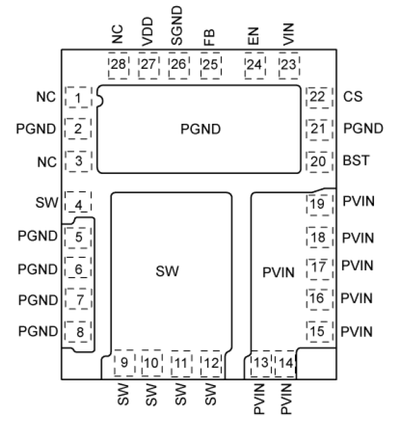
| 13, 14, 15, 16, 17, 18, 19 | PVIN | High-Side Internal N-Channel MOSFET Drain Connection (Input): The
PVIN operating voltage range is from 4.5V to 26V. Input capacitors between the PVIN
pins and the power ground (PGND) are required. Note that the connections must be kept
short. |
| 24 | EN | Enable (Input): A logic level control of the output. The EN pin
is CMOS-compatible. Logic high or floating = enable, logic low = shutdown. In the off
state, the VDD supply current of the device is reduced (typically 0.7mA). |
| 25 | FB | Feedback (Input): Input to the transconductance amplifier of the
control loop. The FB pin is regulated to 0.8V. A resistor divider connecting the
feedback to the output is used to adjust the desired output voltage. |
| 26 | SGND | Signal Ground. SGND must be connected directly to the ground
planes. Do not route the SGND pin to the PGND Pad on the top layer. See the PCB Layout Guidelines section for details. |
| 27 | VDD | VDD Bias (Input): Power to the internal reference and control
sections of the MIC26400. The VDD operating voltage range is from 4.5V to 5.5V. A
2.2μF ceramic capacitor from the VDD pin to SGND must be placed next to the
IC. |
| 2, 5, 6, 7, 8, 21 | PGND | Power Ground. PGND is the ground path for the MIC26400 buck
converter power stage. The PGND pin connects to the source of the low-side N-Channel
internal MOSFET, the negative terminals of input capacitors, and the negative
terminals of output capacitors. The loop for the power ground should be as small as
possible and separate from the Signal Ground (SGND) loop. |
| 22 | CS | Current Sense (Input): High current output driver return. The CS
pin connects directly to the switch node. Due to the high speed switching on this pin,
the CS pin should be routed away from sensitive nodes. CS pin also senses the current
by monitoring the voltage across the low-side internal MOSFET during OFF-time. |
| 20 | BST | Bootstrap (Input): Bootstrapped voltage to the high-side
N-channel internal MOSFET driver. A Schottky diode is connected between the VDD pin
and the BST pin. A boost capacitor of 0.1μF is connected between the BST pin and the
SW pin. |
| 4, 9, 10, 11, 12 | SW | Switch Node (Output): Internal connection for the high-side
MOSFET source and low-side MOSFET drain. |
| 23 | VIN | Power Supply Voltage (Input): Requires a bypass capacitor to
PGND. |
| 1, 3, 28 | NC | No Connect. |