
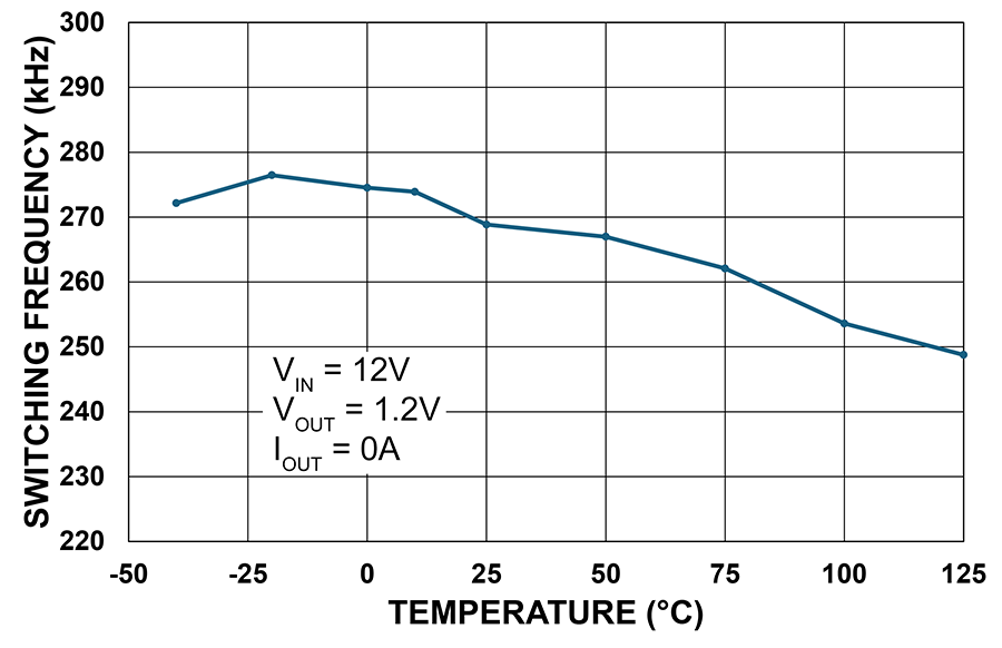
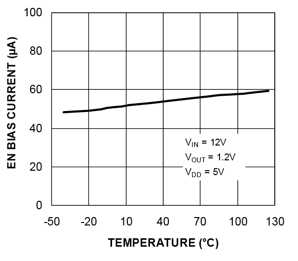
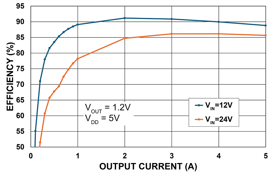
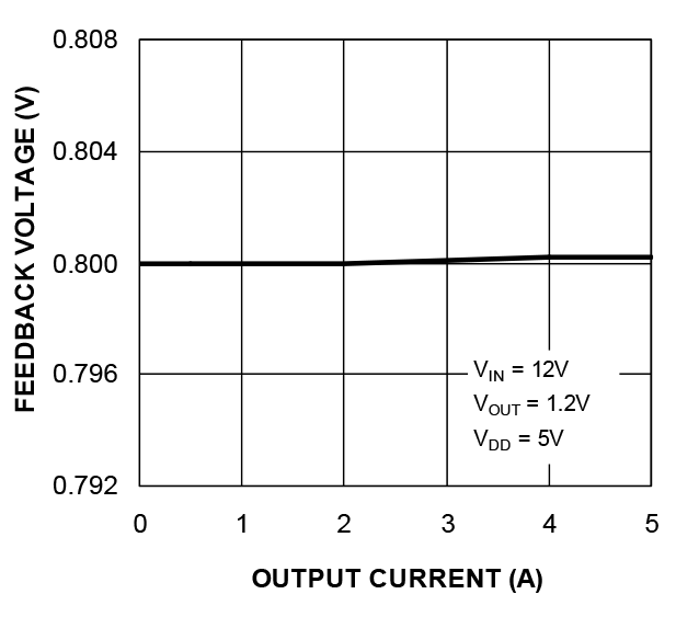
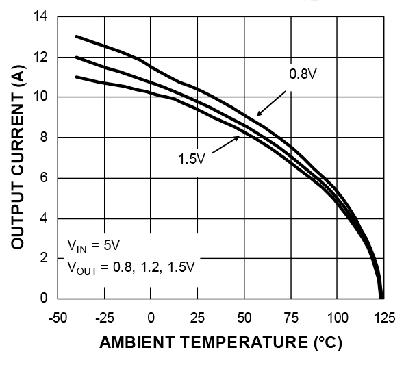
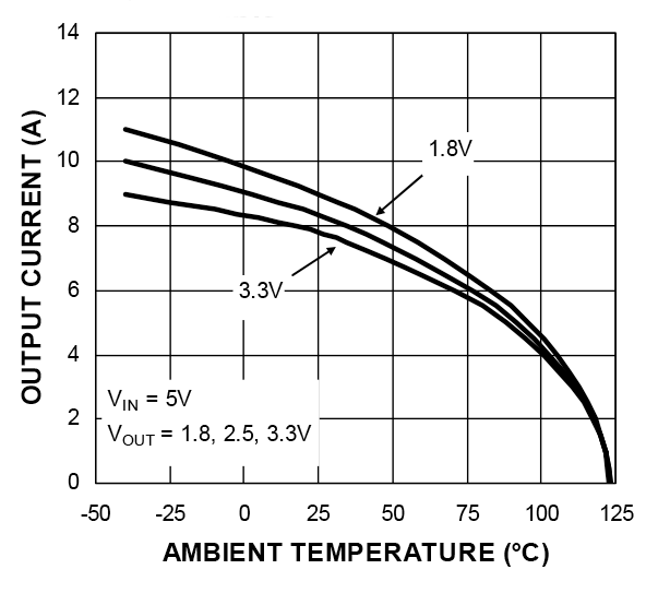
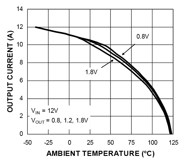
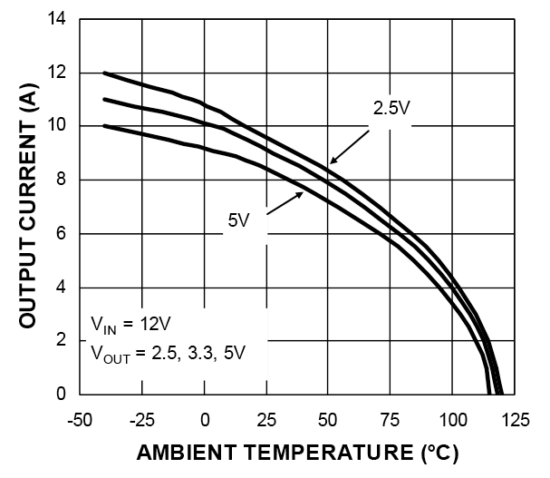
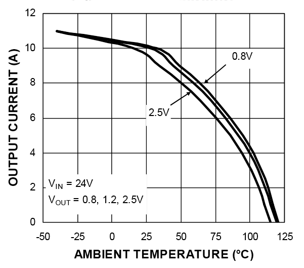
2 Typical Operating Characteristics
Note: The graphs and tables provided following this note are a statistical
summary based on a limited number of samples and are provided for informational purposes only.
The performance characteristics listed herein are not tested or guaranteed. In some graphs or
tables, the data presented may be outside the specified operating range (e.g., outside
specified power supply range) and therefore outside the warranted range.
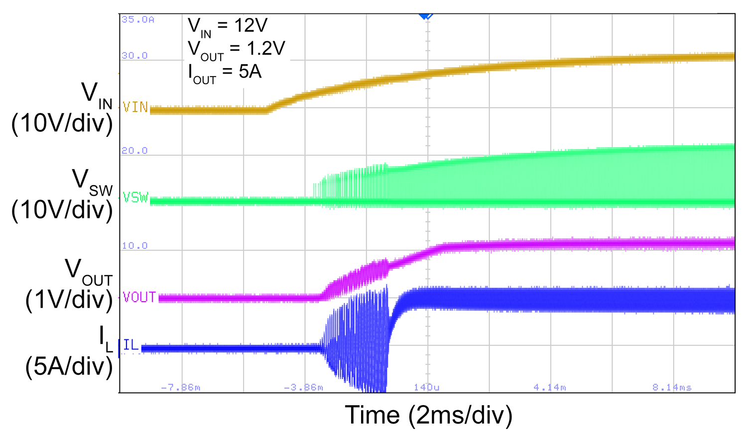
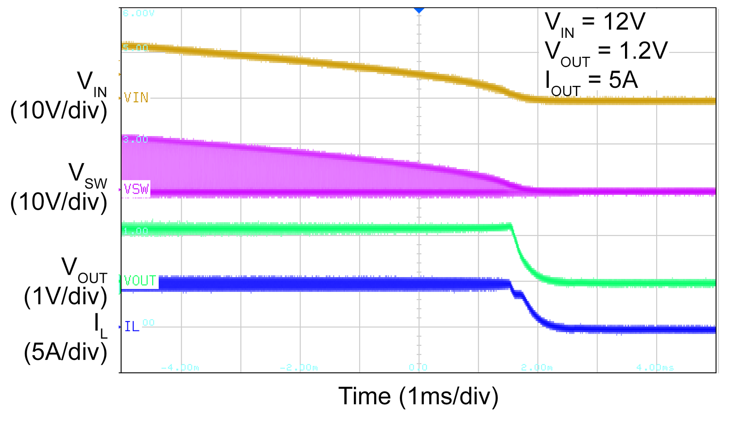
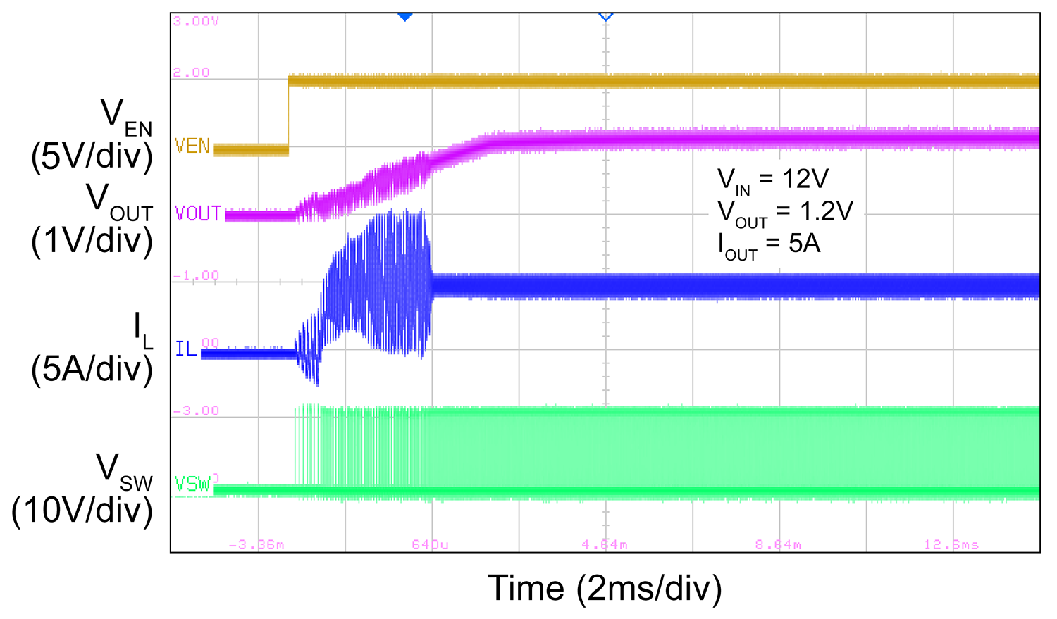
Note: All tests have been performed without the RC Snubber. Please refer
to the Evaluation Board Schematic.
|
|
|
|
|
|
|
|
|
|
|
|
|
|
|
|
|
|
|
|
|
|
|
|
|
|
|
|
|
|
|
|
|
|
|
|
|
|
|
|
|
|
|
|
|
|
|
|
|
|
|
|
|
|
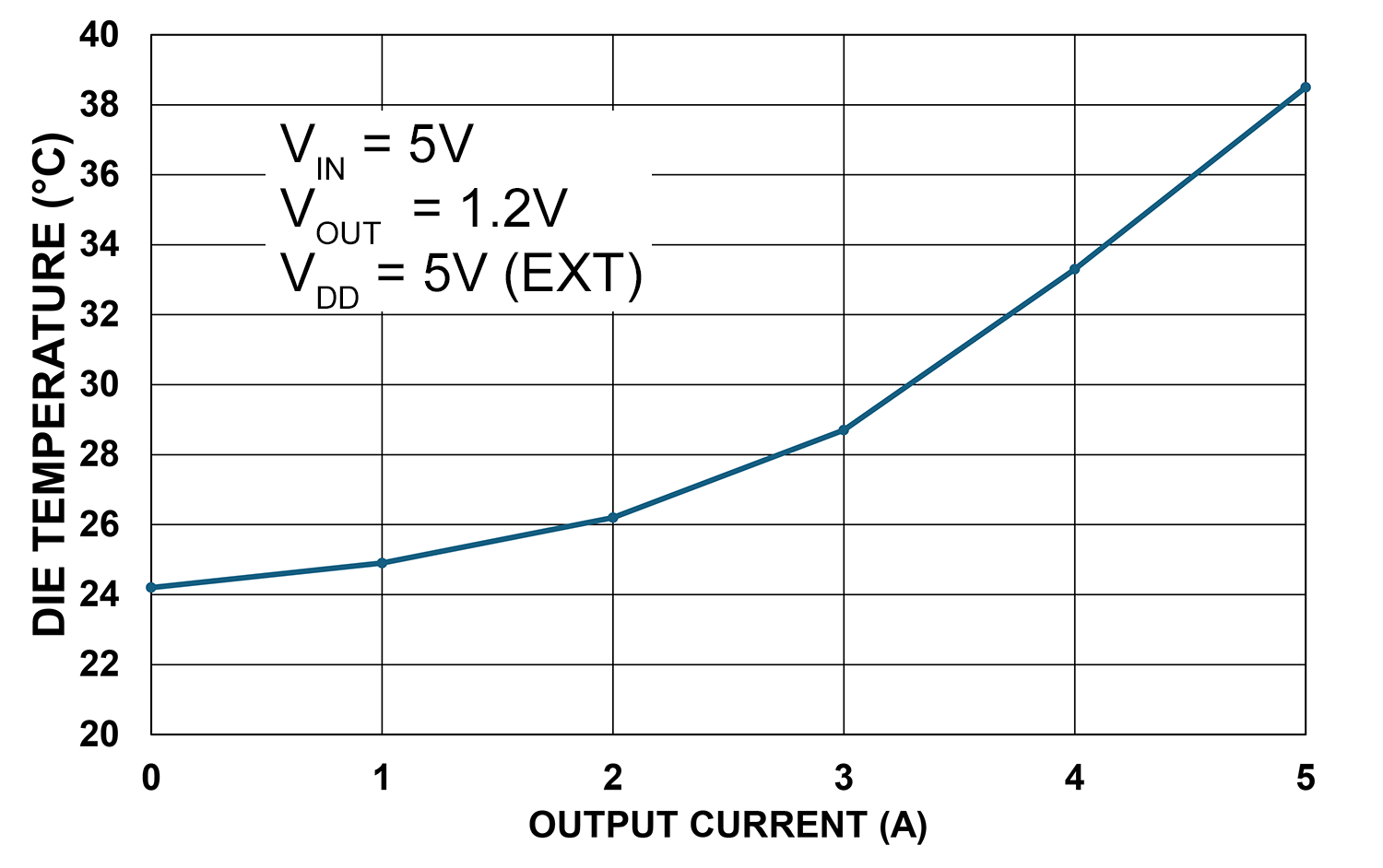
Notes:
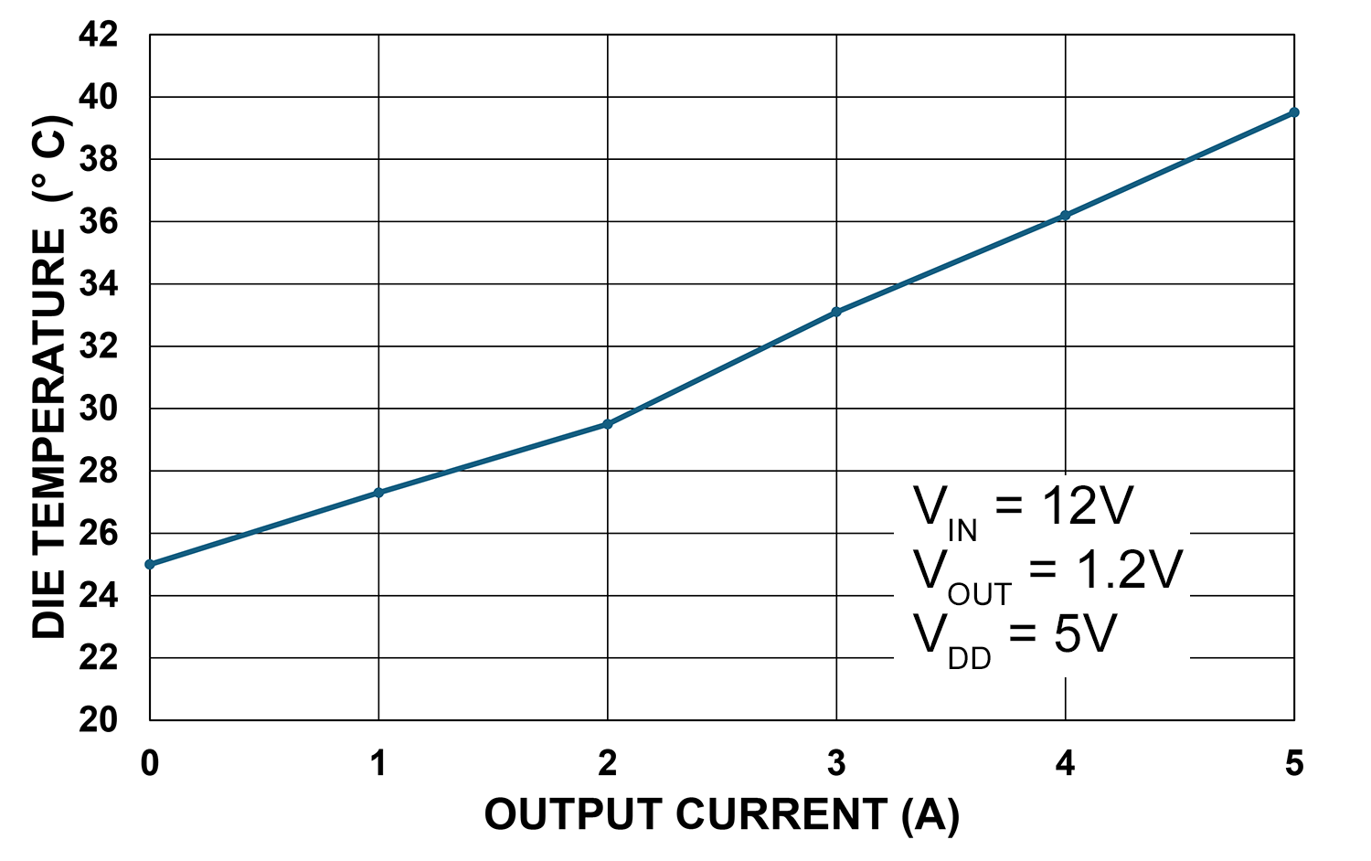
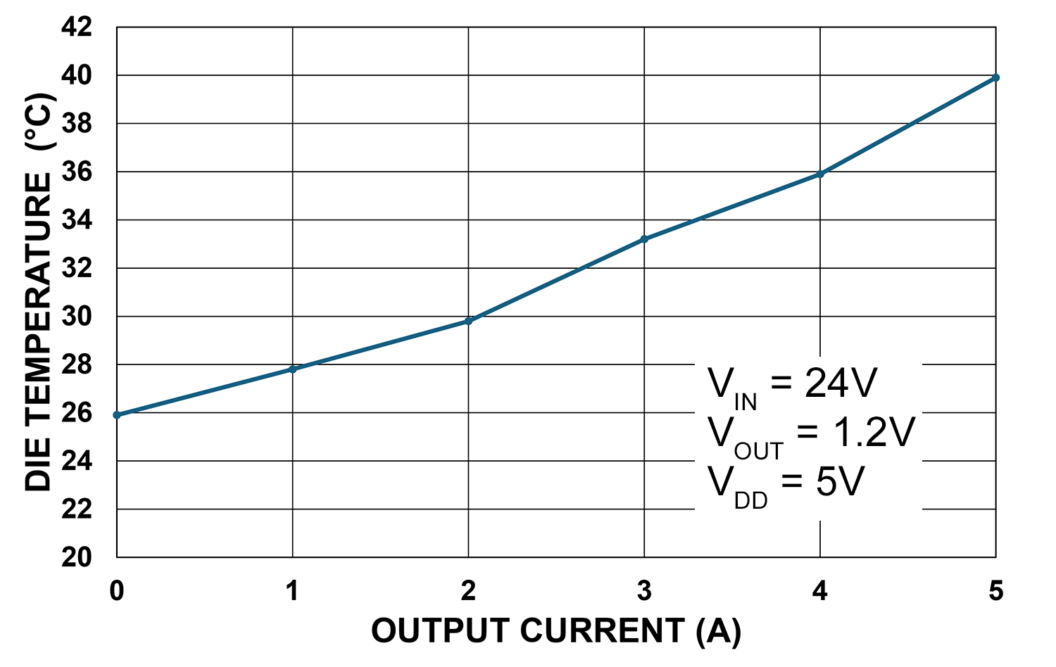
- The temperature measurement was taken at the hottest point on the MIC26400 case mounted on a 5 square inch 4-layer, 0.062”, FR-4 PCB with 2oz. finish copper weight per layer, see the Thermal Measurements section. Actual results will depend upon the size of the PCB, ambient temperature, and proximity to other heat emitting components.