4 Running the Demo
(Ask a Question)This chapter describes how to run the system services demo using the serial terminal program (PuTTY). The prerequisite for the following procedure is to program the device and to set up the serial terminal. For more information on setting up the serial terminal, see Setting up the Serial Terminal Program - PuTTY.
To run the demo, perform the following steps:
-
Power on the board using the SW3 slide switch.
System services options are displayed on the PuTTY, see the following figure.
Figure 4-1. System Services Options 
- Enter 1 to select Read Device
Serial number.
The 128-bit Device Serial Number (DSN) is displayed, see the following figure.
Figure 4-2. Device Serial Number 
Each PolarFire FPGA device has a unique, publicly readable, 128-bit DSN. The DSN can be used in cryptographic protocols to uniquely identify the device. The DSN comprises two 64-bit fields: FSN and SNM.
Factory Serial Number (FSN)—The first (most significant) field is the FSN. It is a pseudo-random per-device unique value assigned during Microchip's manufacturing test and persists for the lifetime of the device.
Serial Number Modifier (SNM)—The second component is the SNM. It is initialized during the factory test and is destroyed during the recoverable zeroization action. If the device is subsequently recovered, a new SNM is assigned such that each SNM generated for a given FSN, is unique.
Important: The system services main menu is displayed after the execution of any of the options. - Enter 2 to select Read Device
User-code.
The 32-bit device USERCODE/Silicon signature is displayed, see the following figure.
Figure 4-3. Device User-code 
This can be configured from
Design flow->Program
                  and Debug Design->Configure Programming Options
. - Enter 3 to select Read Device
Design-info.
See Figure 4-4, the device design information consists of:
- 256-bit user-defined Design ID
- 16-bit design version
This can be configured from
Design flow->Program and Debug Design->Configure Programming
                        Options
. In auto update programming, the current design version is compared with the available images in external SPI flash to initiate the auto update on power up. - 16-bit design back-level
This can be configured from
Design flow->Program and Debug Design->Configure
                        Security
. When back level protection is enabled, the device can only be programmed if the target design version is more than the back level value.Figure 4-4. Device Design Information 
- Enter 4 to select Read Device
Certificate.
The device supply chain assurance certificate is displayed, see Figure 4-5.
For more information about decoding the device certificate, see Appendix 2: Device Certificate Information.
Figure 4-5. Device Certificate 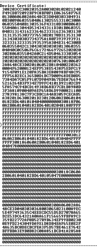
- Enter 5 to select Read Digest.
The 416 byte Digest contains the fabric digest, sNVM digest, and user key digests. The Digest protects data integrity. The following figure shows the 416 byte digest displayed. For more information about decoding the digest output, see Appendix 5: Digest Information
Figure 4-6. Digest 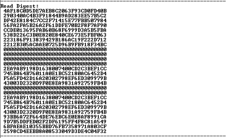
- Enter 6 to select Query
Security.
The non-volatile states of user security locks are displayed, see the following figure.
Figure 4-7. Security Locks Information 
The design does not include any security settings for device safety. Security locks can be configured from
Design flow->Program and
                  Debug Design->Configure Security
. For more information about security locks, see Appendix 2: Device Certificate Information.Important: If security locks are not handled properly, the device can go into the locked state. - Enter 7 to select Read debug
information.
The debug information is displayed, see the following figure.
Figure 4-8. Debug Information 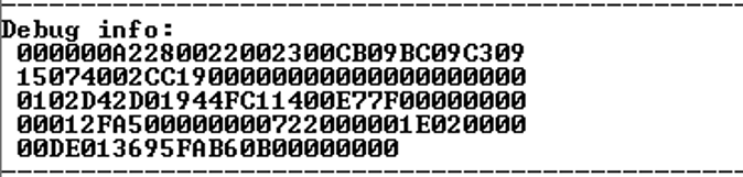
In Figure 4-8, the highlighted 4 bytes E7000000 (LSB first) indicates the number of times (in this example,0x000000E7), the device was programmed (programming cycles). For more information about the Debug Info fields, see Appendix 2: Device Certificate Information.
- Enter 8 to select Digital
Signature.
The following figure displays digital signature in both Raw and DER formats.
Figure 4-9. Digital Signature 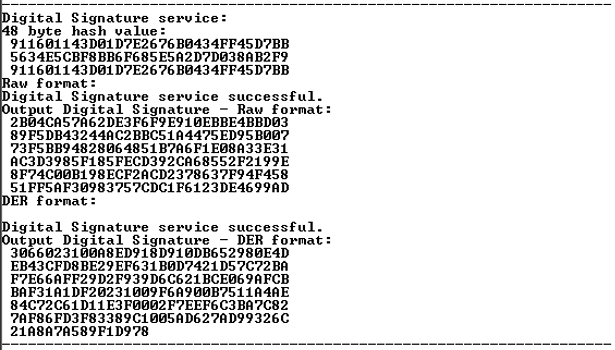
The digital signature service takes a user-supplied SHA384 hash and signs it with the devices private key. The application randomly generates the SHA384 hash value. The Digital Signature service sends the hash value to the System Controller. The Athena core runs the Elliptic Curve Digital Signature Algorithm (ECDSA) using the hash and the device private key to generate the signature.
- Enter 9 to select Secure
NVM.
When the sNVM page/ module address is entered (in this case, 0), the randomly generated 60 byte data is written to the specified sNVM page and read back, see Figure 4-10.
Figure 4-10. Secure NVM Services 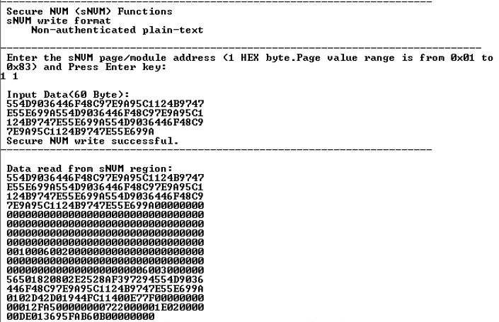
- Enter ‘a’ (without quotes) to select
PUF Emulation_service
The PUF emulation service provides a mechanism for authenticating a device, or for generating a pseudo random bit strings that can be used for different purposes. When this service is selected, the service by default accepts a 128-bit challenge and an 8-bit optype, and returns a 256-bit response unique to the challenge and the optype, see the following figure.
Figure 4-11. PUF Emulation Service 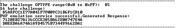
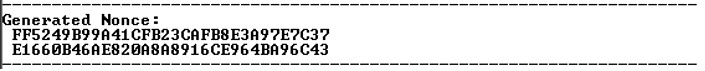
- Enter ‘b’ to select Nonce
service.
The following figure displays 32 byte nonce value. The nonce service provides the ability to strengthen the Deterministic Random Bit Generator (DRBG) of the Athena by providing an alternate entropy source to use as additional seed data in its DRBG functions.
Figure 4-12. Generated Nonce