
4.3 Using R-C From SW Node and Feed-Forward Capacitor (Type 3)
In numerous applications, there is a prevalent demand for power supplies to deliver output with exceedingly low ripple. This requirement is important, especially as many modern applications cannot tolerate more than a 1% ripple-to-output voltage ratio, and output voltages may be less than 1V.
To achieve such stringent ripple requirements, the widespread adoption of very low ESR capacitors, such as ceramic caps, has become commonplace. These capacitors effectively minimize ripple, ensuring that power supplies meet the stringent performance criteria demanded by modern applications.
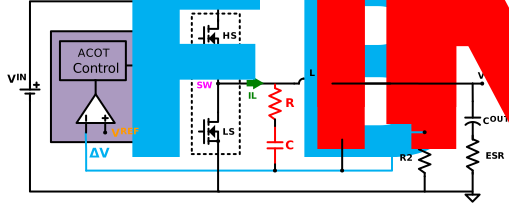
In scenarios where the output ripple is less than 20 – 40 mV (or the minimum limit specified in the data sheet) an alternative ripple injection approach should be employed. A simple and proven method involves deriving ripple from the switched node by utilizing an R-C between the switched node and feedback input, alongside a feed-forward capacitor across the top feedback resistor. The configuration of ripple injection components (RINJ, CINJ, and CFF) is illustrated in Figure 4-7.
The current passing through RINJ is nearly a square wave with no DC component, as blocked by CINJ. This current is then integrated across capacitor CFF to generate a triangular waveform. However, caution must be exercised because CFF also directs the entire “out-of-phase” output ripple to the feedback pin. Therefore, the self-injected “in-phase” ripple must be sufficiently large to overcome the capacitive component of the output ripple.
Feedback Ripple Calculation in Type 3 Ripple Injection
It is beneficial to derive the formula to calculate the ripple voltage expected at the feedback pin using the type 3 ripple injection circuit. As illustrated in Figure 4-8, no net DC current can flow through RINJ in steady state because CINJ can be considered as a DC blocking capacitor. Therefore, the DC (average) values at node SW and at node X must be equal, and the DC (average) value of node SW is D × VIN = VO (assuming a lossless inductor).
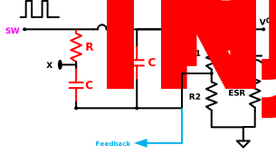
When the SW voltage is equal to VIN, the current injected in the feed-forward capacitor (CFF) is calculated by Figure 3.
Assuming CINJ >> CFF, ensuring CINJ bypasses the high-frequency AC component, and that the impedance of CFF is much smaller than R1 || R2, the ripple current will flow primarily through CFF.
The voltage across a capacitor is given by:
Combining Figure 3 and Figure 4, the peak-to-peak ripple injected to the feedback pin across CFF can be calculated using Figure 5.
This can be rewritten as:
Figure 6 highlights the key parameters that determine the ripple amplitude at the feedback node in the Type-3 ripple-injection network. The ripple magnitude is directly proportional to the input voltage and the duty-cycle factor D(1−D), while it is inversely proportional to the ripple-injection resistance RINJ, the feed-forward capacitor CFF, and the switching frequency.
While it may appear to be a straightforward calculation, when reactive components are introduced into the design, certain conditions must be satisfied to ensure proper operation. For comprehensive design guidelines, please refer to AN7166 - ACOT Design Guide: Control-Loop Analysis and Performance Optimization.