2 Using Basic Logic Gates
This example shows a basic initialization of three CLC peripherals in the Logic Gate mode and how to link to internal peripherals and to I/O ports. The three basic logic functions to take into consideration are: AND, OR and XOR.
The input signals going through the CLC are generated internally by the Timer2, Timer4, PWM3 and PWM4 peripherals. The outputs of the CLC and PWMs are connected to I/O ports for oscilloscope measurements as shown in Figure 2-1.
Setup configurations are the following:
- Timer2 frequency = 100 kHz (10 us period)
- Timer4 frequency = 200 kHz (5 us period)
- PWM3 has Timer2 as source and duty cycle = 50%
- PWM4 has Timer4 as source and duty cycle = 50%
- CLC1 is set up as AND-OR: used as 2-input OR
- CLC2 is set up as 4-input AND: used as 2-input AND
- CLC3 is set up as OR-XOR: used as 2-input XOR
The following are the truth tables and oscilloscope results of each CLC:
- For the OR example (CLC1), two input
signals are used. The truth table is depicted below:
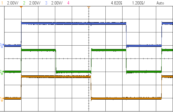
Table 2-1. Truth Table for 2-Input Logic OR Function A B O = A OR B 0 0 0 0 1 1 1 0 1 1 1 1 Figure 2-2 depicts the input and output signals of CLC1 as it performs the OR logic function:
- Signal 1 (Orange) is PWM3 output used as CLC1 Input A
- Signal 2 (Green) is PWM4 output used as CLC1 Input B
- Signal 3 (Blue) is CLC1 output (logic OR between PWM3 and PWM4)
Figure 2-2. Oscillograms of CLC1 Performing Logic OR, Input Signals PWM3 and PWM4 
- For the AND example, two input
signals are used (the CLC in AND mode can have up to four inputs). The truth table
is shown below:
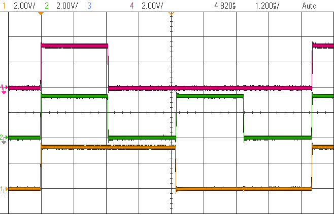
Table 2-2. Truth Table for 2-Input Logic AND Function A B O = A AND B 0 0 0 0 1 0 1 0 0 1 1 1 Figure 2-3 depicts the input and output signals of CLC2 as it performs the AND logic function:
- Signal 1 (Orange) is PWM3 output used as CLC2 Input A
- Signal 2 (Green) is PWM4 output used as CLC2 Input B
- Signal 4 (Red) is CLC2 output (logic AND between PWM3 and PWM4)
Figure 2-3. Oscillograms of CLC2 Performing Logic AND, Input Signals PWM3 and PWM4 
- For the XOR example, two input
signals are used. The truth table is shown below:
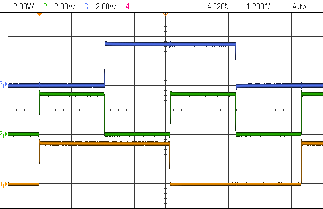
Table 2-3. Truth Table for 2-Input Logic XOR Function A B O = A XOR B 0 0 0 0 1 1 1 0 1 1 1 0 Figure 2-4 depicts the input and output signals of CLC3 as it performs the XOR logic function:
- Signal 1 (Orange) is PWM3 output used as CLC3 Input A
- Signal 2 (Green) is PWM4 output used as CLC3 Input B
- Signal 3 (Blue) is CLC3 output (logic XOR between PWM3 and PWM4)
Figure 2-4. Oscillograms of CLC3 Performing Logic XOR, Input Signals PWM3 and PWM4 
- System clock initialization
- Port initialization
- Timer initialization
- PWM initialization
- CLC initialization.
