3 Using CLCs to Create a Data Signal Modulator (DSM)
This example shows an initialization of the CLC in the J-K flip-flop with R mode and AND-OR mode for the implementation of a Data Signal Modulator (DSM) with timings controlled from the CCP peripheral. The truth table of the J-K flip-flop is shown below.
| CLK | J | K | O |
|---|---|---|---|
| 0 | 0 | 0 | Latch |
| 0 | 0 | 1 | 0 |
| 0 | 1 | 0 | 1 |
| 0 | 1 | 1 | Toggle |
| 1 | 0 | 0 | Latch |
| 1 | 0 | 1 | Latch |
| 1 | 1 | 0 | Latch |
| 1 | 1 | 1 | Latch |
CLC1 (J-K flip-flop 1) has Timer2 as clock source (which represents the first modulated frequency), while the carrier signal generated from the CCP is connected to the J gate of the J-K flip-flop. The K gate is left to logic 1. This allows the CLC to toggle when the J input is high and stay 0 when the J input is low.
CLC2 (J-K flip-flop 2) is connected in the same way with Timer4 as clock source and the negated CCP as input for the J gate. This CCP connection to the J gates ensures that one CLC is toggling while the other has the output set to 0 logic. CLC3 set in AND-OR mode is connecting CLC1 and CLC2 outputs to create a DSM.
The internal architecture is shown in Figure 3-1.
DSM setup configurations:
- Timer2 frequency = 1 MHz (1 us period)
- Timer4 frequency = 500 kHz (2 us period)
- Timer6 frequency = 62.5 kHz (16 us period)
- CCP1 has Timer6 as source and duty cycle = 50%
- CLC1 is set up as J-K flip-flop with R
- CLC2 is set up as J-K flip-flop with R
- CLC3 is set up as AND-OR: used as 2-input OR
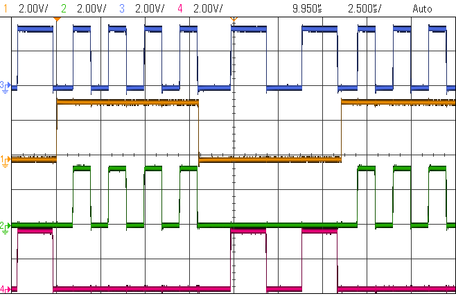
Figure 3-2 displays all the CLCs outputs and the CCP1 output side by side to show how this configuration implements the DSM function:
- Signal 1 (Orange) is CCP1 output
- Signal 2 (Green) is CLC1 output
- Signal 3 (Blue) is CLC3 output
- Signal 4 (Red) is CLC2 output

- System clock initialization
- Port initialization
- Timer initialization
- CCP initialization
- CLC initialization.
