1 Electrical Characteristics

Table 1-1. Absolute Maximum Ratings
ParameterSymbolValue
Storage TemperatureTS–55°C to +125°C
Soldering Temperature/TimeTLS260°C / 10 sec.
Supply VoltageVDD–0.3V to +4.5V
Note: Stresses in excess of the absolute maximum ratings can permanently damage the device. Functional operation is not implied at these or any other conditions in excess of the conditions represented in the operational sections of this data sheet. Exposure to absolute maximum ratings for extended periods may adversely affect device reliability. Permanent damage is also possible if E/D is applied before VDD.
Table 1-2. ESD Ratings
ModelMinimumConditions
Human Body Model2000VMIL-STD-883, Method 3015
Charged Device Model750VJESD22-C101
Note: Although ESD protection circuitry has been designed into the VC-870, proper precautions should be taken when handling and mounting. Microchip employs a human body model (HBM) and a charged device model (CDM) for ESD susceptibility testing and design protection evaluation.
Table 1-3. 3.3V Electrical Performance
ParameterSymbolMin.Typ.Max.UnitsConditions
Supply
VoltageVDD3.03.33.6VNote 1
Maximum VoltageVDD(MAX)–0.34.5V
CurrentIDD2.4mA≤40.000MHz, Note 2
4.2>40.000MHz, Note 2
10µAOutput Disabled
Frequency
Nominal FrequencyfNOM0.5487580MHz
StabilityfSTAB±25ppmOrdering Option
±50
±100
Outputs
Output Logic Level HighVOH0.9 x VDDVNote 2
Output Logic Level LowVOL0.1 x VDDVNote 2
LoadCLOAD15pF
Output Rise/Fall TimetR/tF3nsNote 2
Duty CycleDC455055%Note 3
Period Jitter, RMSΦJ2.2ps
Period Jitter, Peak-to-Peak20ps
Enable/Disable
Output EnableVIH0.7 x VDDVNote 4
Output DisableVIL0.3 x VDDVNote 4
Disable TimetDIS200ns
Start-Up TimetSU2ms
Operating TemperatureTOP–20+70°COrdering Option
–40+85°C
Notes:
  1. The power supply should have bypass capacitors as close to the supply and to ground as possible (for example, 0.1µF and 0.01µF).
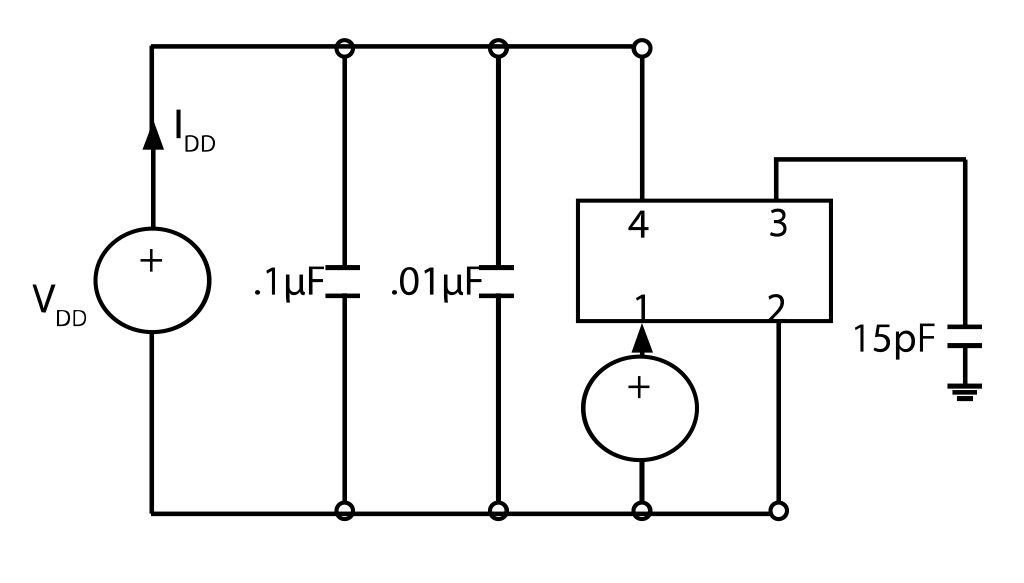
  2. Parameters are tested with the production test circuit in Figure 1-1.
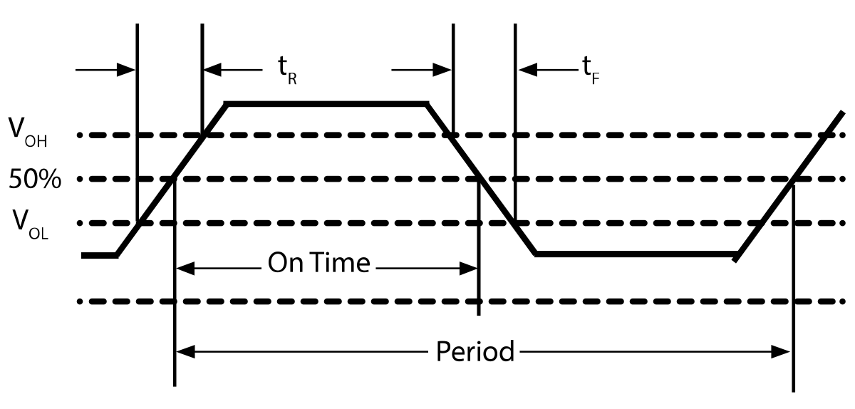
  3. Duty Cycle is measured as On-Time/Period (see Figure 1-2).
  4. A 10kΩ pull-up resistor to VDD is recommended if the E/D pin is unused.
Table 1-4. 2.5V Electrical Performance
ParameterSymbolMin.Typ.Max.UnitsConditions
Supply
VoltageVDD2.252.52.75VNote 1
Maximum VoltageVDD(MAX)–0.34.5V
CurrentIDD2.0mA≤40.000MHz, Note 2
3.4>40.000MHz, Note 2
10µAOutput Disabled
Frequency
Nominal FrequencyfNOM0.5487580MHz
StabilityfSTAB±25ppmOrdering Option
±50
±100
Outputs
Output Logic Level HighVOH0.9 x VDDVNote 2
Output Logic Level LowVOL0.1 x VDDVNote 2
LoadCLOAD15pF
Output Rise/Fall TimetR/tF5nsNote 2
Duty CycleDC455055%Note 3
Period Jitter, RMSΦJ2.2ps
Period Jitter, Peak-to-Peak20ps
Enable/Disable
Output EnableVIH0.7 x VDDVNote 4
Output DisableVIL0.3 x VDDVNote 4
Disable TimetDIS150ns
Start-Up TimetSU2ms
Operating TemperatureTOP–20+70°COrdering Option
–40+85°C
Notes:
  1. The power supply should have bypass capacitors as close to the supply and to ground as possible (for example, 0.1µF and 0.01µF).
  2. Parameters are tested with the production test circuit in Figure 1-1.
  3. Duty Cycle is measured as On-Time/Period (see Figure 1-2).
  4. A 10kΩ pull-up resistor to VDD is recommended if the E/D pin is unused.
Table 1-5. 1.8V Electrical Performance
ParameterSymbolMin.Typ.Max.UnitsConditions
Supply
VoltageVDD1.61.82.0VNote 1
Maximum VoltageVDD(MAX)–0.34.5V
CurrentIDD4.0mA≤40.000MHz, Note 2
6.0>40.000MHz, Note 2
10µAOutput Disabled
Frequency
Nominal FrequencyfNOM0.5478580MHz
StabilityfSTAB±25ppmOrdering Option
±50
±100
Outputs
Output Logic Level HighVOH0.9 x VDDVNote 2
Output Logic Level LowVOL0.1 x VDDVNote 2
LoadCLOAD15pF
Output Rise/Fall TimetR/tF5nsNote 2
Duty CycleDC455055%Note 3
Period Jitter, RMSΦJ2.2ps
Period Jitter, Peak-to-Peak20ps
Enable/Disable
Output EnableVIH0.7 x VDDVNote 4
Output DisableVIL0.3 x VDDVNote 4
Disable TimetDIS200ns
Start-Up TimetSU2ms
Operating TemperatureTOP–20+70°COrdering Option
–40+85°C
Notes:
  1. The power supply should have bypass capacitors as close to the supply and to ground as possible (for example, 0.1µF and 0.01µF).
  2. Parameters are tested with the production test circuit in Figure 1-1.
  3. Duty Cycle is measured as On-Time/Period (see Figure 1-2).
  4. A 10kΩ pull-up resistor to VDD is recommended if the E/D pin is unused.
Figure 1-1. Test Circuit
Figure 1-2. Waveform