LVDS
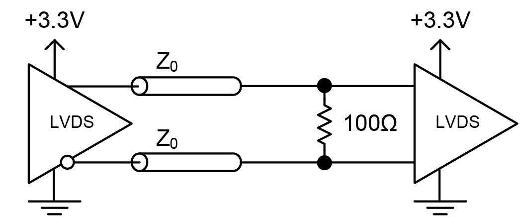
LVDS stands for Low Voltage Differential Signaling and is similar to LVPECL being a current output. However, the output current is 4mA, which results in lower power consumption compared to LVPECL. LVDS outputs have a 100Ω output impedance and is meant to drive a 100Ω load or resistor. This results in smaller voltage swings, typically ~350mV.
LVDS maintains reduced susceptibility to noise and lower EMI emissions compared to CMOS and TTL. A disadvantage of LVDS can be its reduced jitter performance compared to PECL; however, advances are being made to put it on a level playing field with LVPECL.
LVDS is used in high speed data transfer applications; in particular, backplane transceivers or clock distribution. LVDS operates at data rates up to 3.125Gbps. For higher data rates, outputs such as HCSL, CML, or LVPECL are required. Achieving these very high data rates requires very fast, sharp-edge rates and typically a signal swing of approximately 800mV. Because of this, HCSL, CML, and LVPECL generally require more power than LVDS.
LVDS is typically chosen for newer designs because of its ease of implementation in CMOS ICs, lower power, and because of its ease of use at the system level. LVDS outputs require no external biasing and a single 100Ω termination resistor when connected to LVDS inputs, see Figure . The LVDS signal may or may not need to be AC-coupled after the 100Ω load. It is always best to understand the receiver’s input structure requirements.