
3.3.3 NAND Flash Memory
The SAMA7G54 Curiosity Pro board features one 4 Gb SLC NAND Flash memory device: MX30LF4G28AD-XKI.
The high capacity of this memory device enables storage of large programs and operating systems.
The SAMA7G54 MPU features one Programmable Multibit Error Correcting Code (PMECC) controller, which can be used to generate redundancy information for both SLC and MLC NAND devices. It supports redundancy for the correction of 2, 4, 8, 12, 24 or 32 errors per data sector.
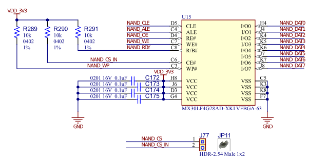
Keep the JP11 jumper placed on the J77 header to enable booting from or using the NAND Flash memory.
Remove the JP11 jumper to prevent the system from booting from the NAND Flash memory.
| PIO | Signal Name | Signal Description |
|---|---|---|
| PD2 | NAND_DAT7 | NAND Flash data 7 |
| PD3 | NAND_RDY | NAND Flash Ready signal |
| PD4 | NAND_CS_IN | NAND Flash chip select line |
| PD5 | NAND_WE | NAND Flash Write Enable signal |
| PD6 | NAND_OE | NAND Flash Output Enable signal |
| PD7 | NAND_ALE | NAND Flash Address Latch Enable signal |
| PD8 | NAND_CLE | NAND Flash Command Latch Enable signal |
| – | NAND_WP | NAND Flash Write Protect |
| PD9 | NAND_DAT0 | NAND Flash data 0 |
| PD10 | NAND_DAT1 | NAND Flash data 1 |
| PD11 | NAND_DAT2 | NAND Flash data 2 |
| PC21 | NAND_DAT3 | NAND Flash data 3 |
| PC22 | NAND_DAT4 | NAND Flash data 4 |
| PC23 | NAND_DAT5 | NAND Flash data 5 |
| PC24 | NAND_DAT6 | NAND Flash data 6 |